

Semiconductor device, production method thereof, and display device
a semiconductor and display device technology, applied in semiconductor devices, electrical equipment, instruments, etc., can solve the problems of damage to the gate electrode formed on the semiconductor thin film in the pixel part, and achieve the effects of reducing the parasitic capacitance, reducing the electric power consumption, and low electric power consumption
- Summary
- Abstract
- Description
- Claims
- Application Information
AI Technical Summary
Benefits of technology
Problems solved by technology
Method used
Image

Examples
embodiment 1
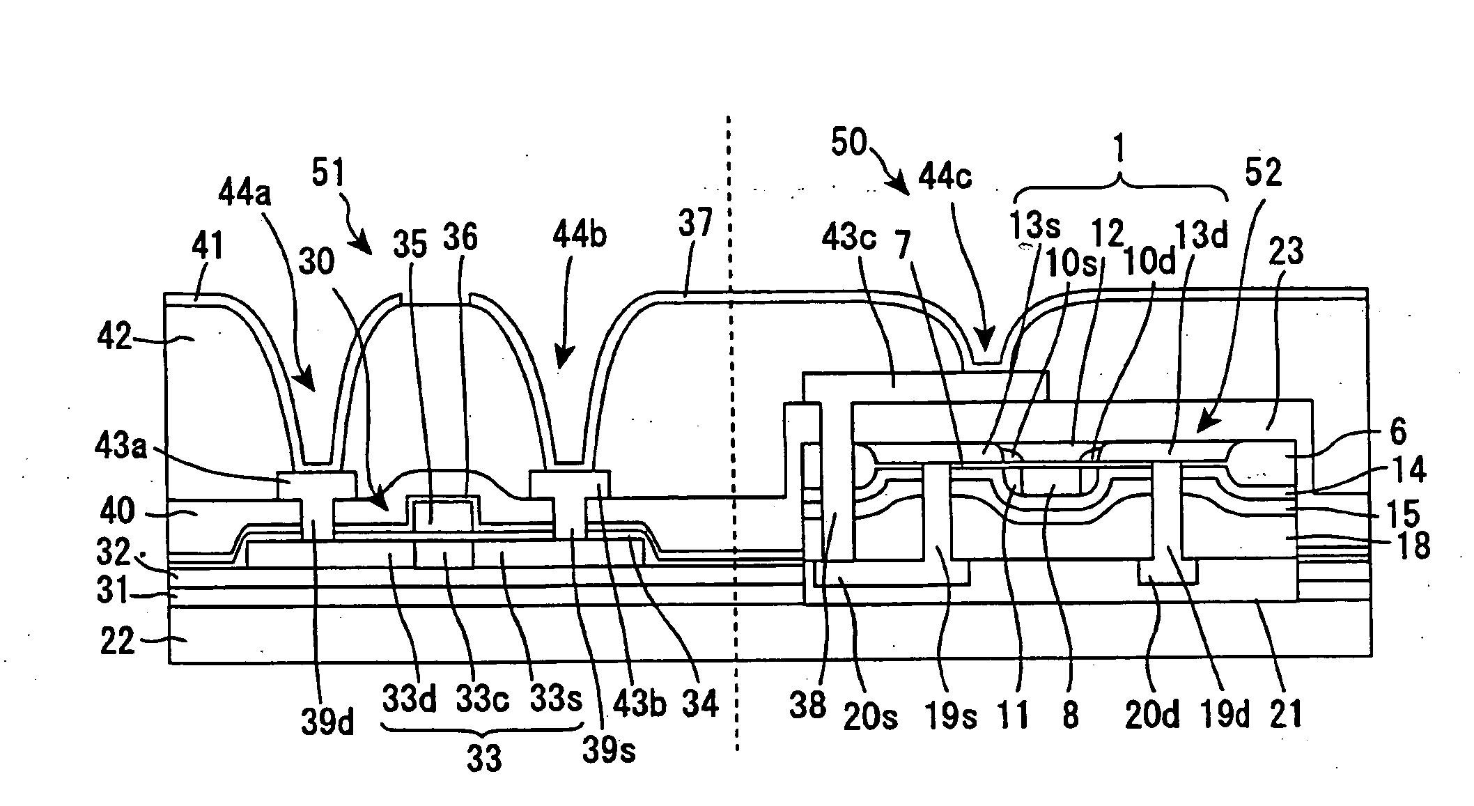
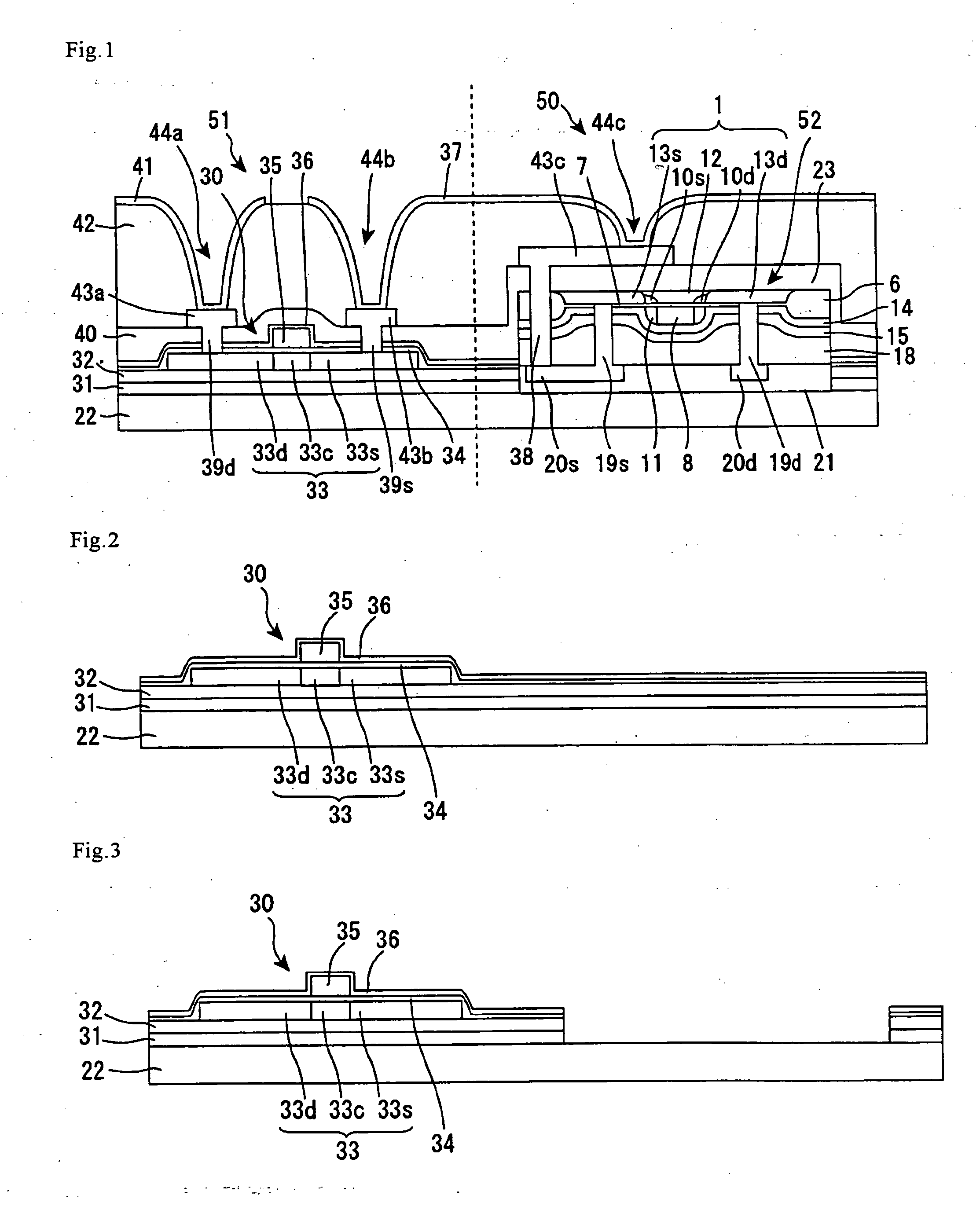
[0047]An active matrix substrate for display devices, including the semiconductor device of the present invention, is mentioned with reference to FIG. 1. FIG. 1 is a cross-sectional view schematically showing a configuration of an active matrix substrate for display devices, in accordance with the present Embodiment. As shown in FIG. 1, the active matrix substrate in the present Embodiment includes a glass substrate 22 that is a transparent substrate, an IC part 50 and a pixel part 51 each arranged on the glass substrate 22, and a wiring part 37 connecting a TFT 30 in the pixel part 51 to the IC part 50.
[0048]The pixel part 51 includes the TFT 30 on a first base coat layer 31 and a second base coat layer 32 successively formed on the glass substrate 22.
[0049]The TFT 30 includes: a semiconductor thin film 33 including an active region; a gate insulating film 34 covering the semiconductor thin film 33; a gate electrode (gate in the pixel part) 35 formed on the gate insulating film 34;...
PUM
 Abstract
Description
Claims
Application Information