Vertical-type semiconductor devices

Active Publication Date: 2009-10-01
SAMSUNG ELECTRONICS CO LTD
View PDF6 Cites 112 Cited by
  • Summary
  • Abstract
  • Description
  • Claims
  • Application Information

AI Technical Summary

Benefits of technology

[0052]According to some example embodiments, since a vertical-type non-volatile memory device has a structure in which cell transistors are connected in series in a vertical direction, the memory device may be highly integrated. Further, in the vertical non-volatile memory device, the cell transistors are pro

Problems solved by technology

However, further integration of such devices is limited by the substrate dimensions.
However, when the cell transistors included in the flash memory device are formed to be stacked vertically, uniformity between operating characteristics of each of the cell transistors positioned in the vertical direction and operating characteristics of each of the cell transistors formed on the substrate is difficult to achieve.
In particular, when a channel region of the cell transistor is formed using polysilicon, cell distribution characteristics of the cell transistor including polysilicon may be poor and the op

Method used


Image

  • Vertical-type semiconductor devices
  • Vertical-type semiconductor devices
  • Vertical-type semiconductor devices

Examples


Example

Embodiment 1

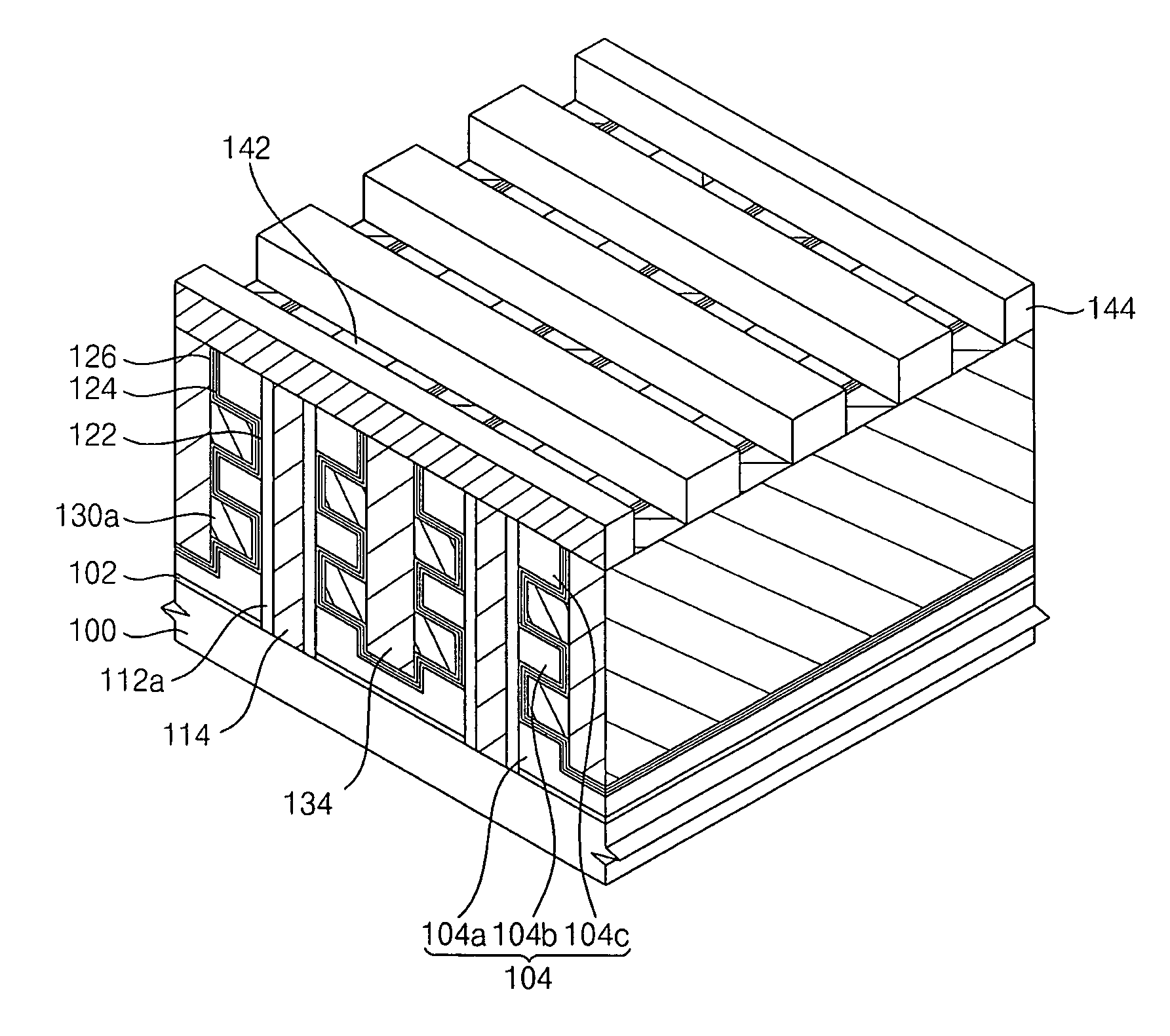
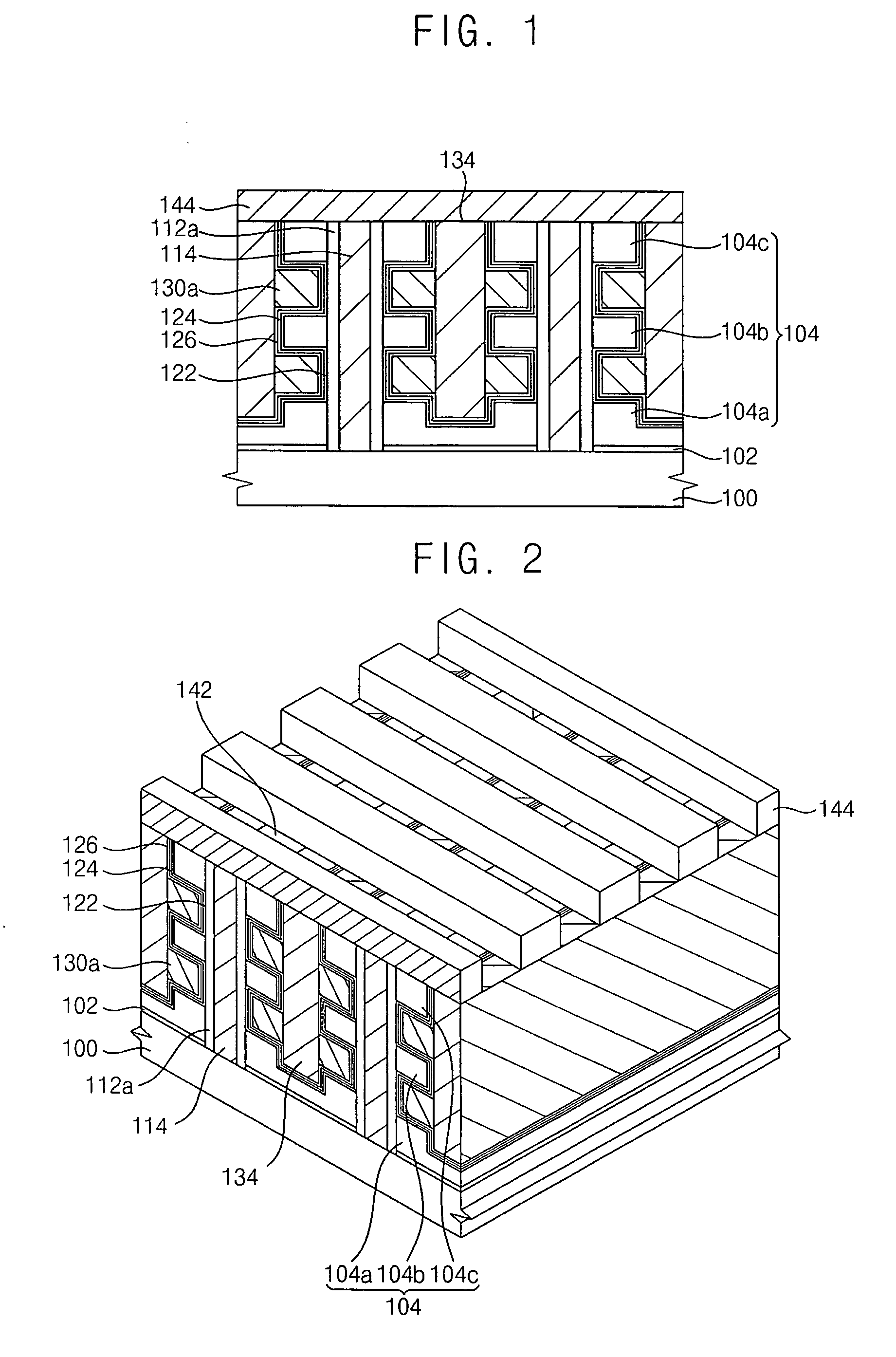
[0075]FIG. 1 is a cross-sectional view illustrating a non-volatile memory device in accordance with a first example embodiment. FIG. 2 is a perspective view illustrating the non-volatile memory device of FIG. 1.

[0076]Referring to FIGS. 1 and 2, a substrate 100 including a single-crystalline semiconductor material is provided. For example, the substrate 100 may include single-crystalline silicon.

[0077]An impurity region (not illustrated) is provided under a surface of the substrate 100 to be provided as a common source line. The impurity region is formed in a portion of the substrate where one cell block is formed. The impurity region may include n-type impurities. The impurity region may be connected to a lower portion of each of cell strings that is formed in a single-crystalline semiconductor pattern 112a.

[0078]An insulation layer pattern 114 is provided on the substrate 100. The insulation layer pattern 114 may have a linear shape extending in a first direction. An u...

Example

Embodiment 2

[0198]FIG. 32 is a cross-sectional view illustrating a vertical-type semiconductor device in accordance with a second example embodiment.

[0199]The semiconductor device of the present embodiment is substantially the same as Embodiment 1 except that a metal-oxide semiconductor (MOS) transistor is formed on a sidewall of a single-crystalline silicon pattern having a pillar shape. That is, the semiconductor device illustrated in FIG. 32 has a structure in which MOS transistors including a gate oxide layer 202 and a gate electrode 204 are connected in series to one another.

[0200]The method of forming a structure of FIG. 32 may be selected from any one of methods of manufacturing a memory device according to Embodiment 1. However, since the charge-trapping layer and the blocking dielectric layer are not required for the MOS transistor, there is only a difference that processes of forming the charge-trapping layer and the blocking dielectric layer are not performed. Thus, any f...

Example

Embodiment 3

[0201]FIG. 33 is a cross-sectional view illustrating a non-volatile memory device in accordance with a third example embodiment. FIG. 34 is a perspective view illustrating the non-volatile memory device of FIG. 33.

[0202]The non-volatile memory device of the present embodiment is substantially the same as Embodiment 1 except that a metal silicide pattern is formed on a surface of a control gate pattern in a non-volatile memory device. Thus, any further explanations with respect to the same elements will be omitted.

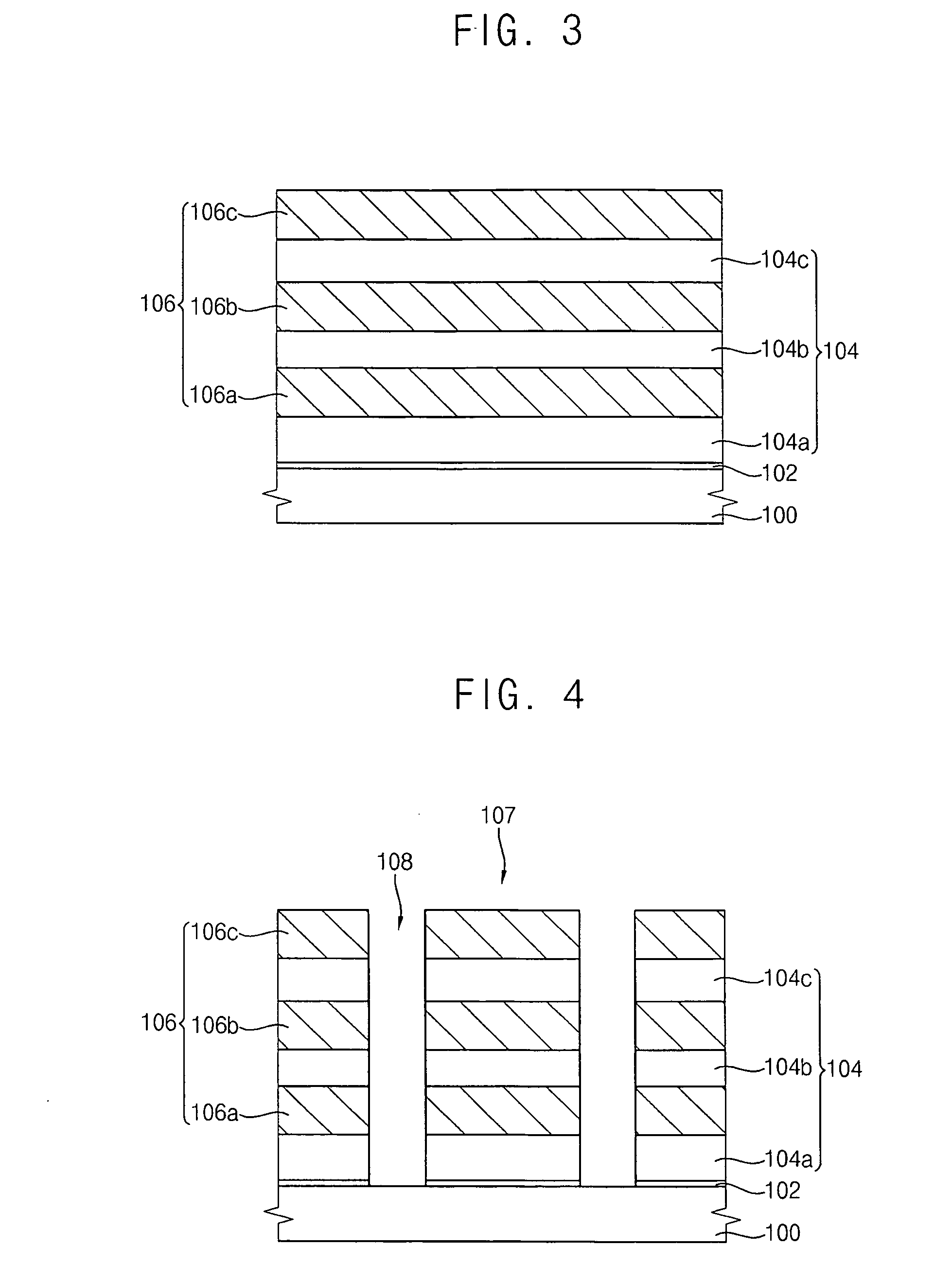
[0203]Referring to FIG. 33, the substrate 100 including a single-crystalline semiconductor material is provided. An impurity region is provided under the surface of the substrate 100 to be provided as a common source line.

[0204]The insulation layer pattern 114 is provided on the substrate 100 to have a linear shape extending in the first direction. The pillar-shaped single-crystalline semiconductor patterns 112a are provided on both the sidewalls of the insulati...


PUM


Abstract

In a vertical-type memory device and a method of manufacturing the vertical-type memory device, the vertical memory device includes an insulation layer pattern of a linear shape provided on a substrate, pillar-shaped single-crystalline semiconductor patterns provided on both sidewalls of the insulation layer pattern and transistors provided on a sidewall of each of the single-crystalline semiconductor patterns. The transistors are arranged in a vertical direction of the single-crystalline semiconductor pattern, and thus the memory device may be highly integrated.

Description

BACKGROUND[0001]1. Field[0002]Example embodiments relate to vertical-type semiconductor devices and methods of manufacturing the same. More particularly, example embodiments relate to semiconductor devices including cells that are connected vertically to one another and a method of manufacturing the same.[0003]2. Description of the Related Art[0004]Semiconductor memory devices can be categorized generally as volatile memory devices, e.g., dynamic random access memory (DRAM) or static random access memory (SRAM), and non-volatile memory devices, e.g., flash memory devices. The degrees of integration, operating speeds and capacitances of the semiconductor memory devices have been greatly improved due to expanding application fields thereof.[0005]From a circuit point of view, a flash memory device of the non-volatile memory devices may be classified as either a NAND-type flash memory device or a NOR-type flash memory device. In the NAND-type flash memory device, unit strings including ...

Claims


Application Information

Patent Timeline
IPC IPC(8): H01L29/792
CPCH01L27/11578H01L27/11582H01L29/66833H01L29/66787H01L29/7926H01L27/1052H01L29/66666H01L29/792H01L29/40117H10B43/20H10B43/27H10B99/00H10B43/30H10B43/23H01L21/02524H01L21/02587H01L21/02598H01L21/02675H01L21/28518H01L21/30604H01L21/32133H01L29/4234H01L29/665H01L29/45
Inventor SON, YONG-HOONLEE, JONG-WOOKKANG, JONG-HYUK
Owner SAMSUNG ELECTRONICS CO LTD
Why Eureka
Try Eureka