Micro integrated planar optical waveguide type spr sensor

a planar optical waveguide and sensor technology, applied in the field of surface plasmon resonance sensors, can solve the problems of device bulkiness, sensor is not fully integrated on a planar surface, reflector spr sensor is “bulky”, etc., and achieve the effect of reducing the size of spr sensors

Inactive Publication Date: 2009-10-01
UNIV OF CENT FLORIDA RES FOUND INC
View PDF6 Cites 29 Cited by
  • Summary
  • Abstract
  • Description
  • Claims
  • Application Information

AI Technical Summary

Benefits of technology

[0011]A first objective of the present invention is to provide methods, systems apparatus and devices that integrate light source and detection system and sensing layer and reduce the size of SPR sensor.
[0012]A second objective of the present invention is to provide methods, systems apparatus and devices to make planar SPR sensor structure and provide the availability of full integration of planar microfluidic components to the substrate.
[0013]A third objective of the present invention is to provide methods, systems apparatus and devices to allow for batch fabrication of the planar integrated optical waveguide type SPR sensor to reduce product cost.
[0014]A fourth objective of the present invention is to provide methods, systems apparatus and devices to make planar simple-structured SPR sensor and provide flexibility in fabrication.
[0015]A fifth objective of the present invention is to provide methods, systems apparatus and devices to remove external optical components and eliminate optical component alignment problem.

Problems solved by technology

However, a disadvantage of the reflector sensor is that the sensor is not fully integrated on a planar surface.
Thus, the reflector SPR sensor is “bulky”.
While the overall size of the reflective SPR sensor is reduced, the resulting device is still bulky.
While the Duveneck device may be enclosed to form a single unit, the device is bulky since the device requires a first substrate for the light source and detector and a separate second substrate for the coupling-in and coupling-out gratings, optical waveguide and corresponding SPR surface area.

Method used


Image

  • Micro integrated planar optical waveguide type spr sensor
  • Micro integrated planar optical waveguide type spr sensor
  • Micro integrated planar optical waveguide type spr sensor

Examples


Embodiment Construction

[0032]Before explaining the disclosed embodiments of the present invention in detail it is to be understood that the invention is not limited in its application to the details of the particular arrangements shown since the invention is capable of other embodiments. Also, the terminology used herein is for the purpose of description and not of limitation.

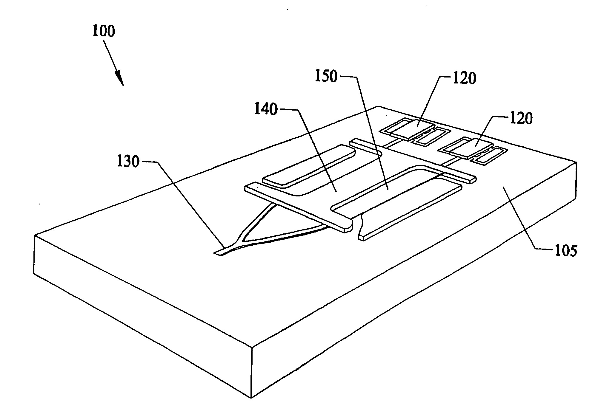
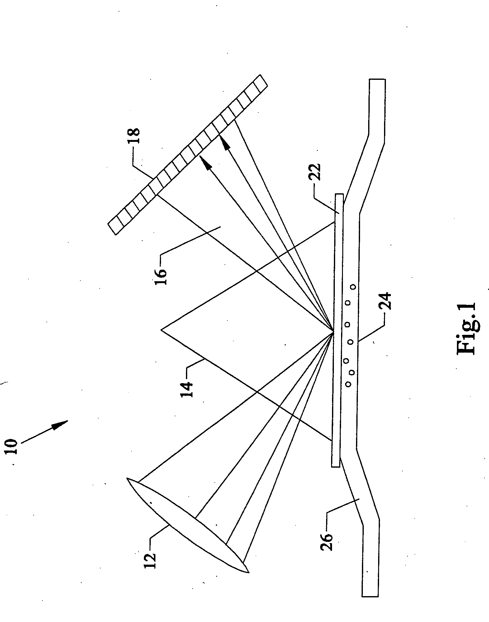
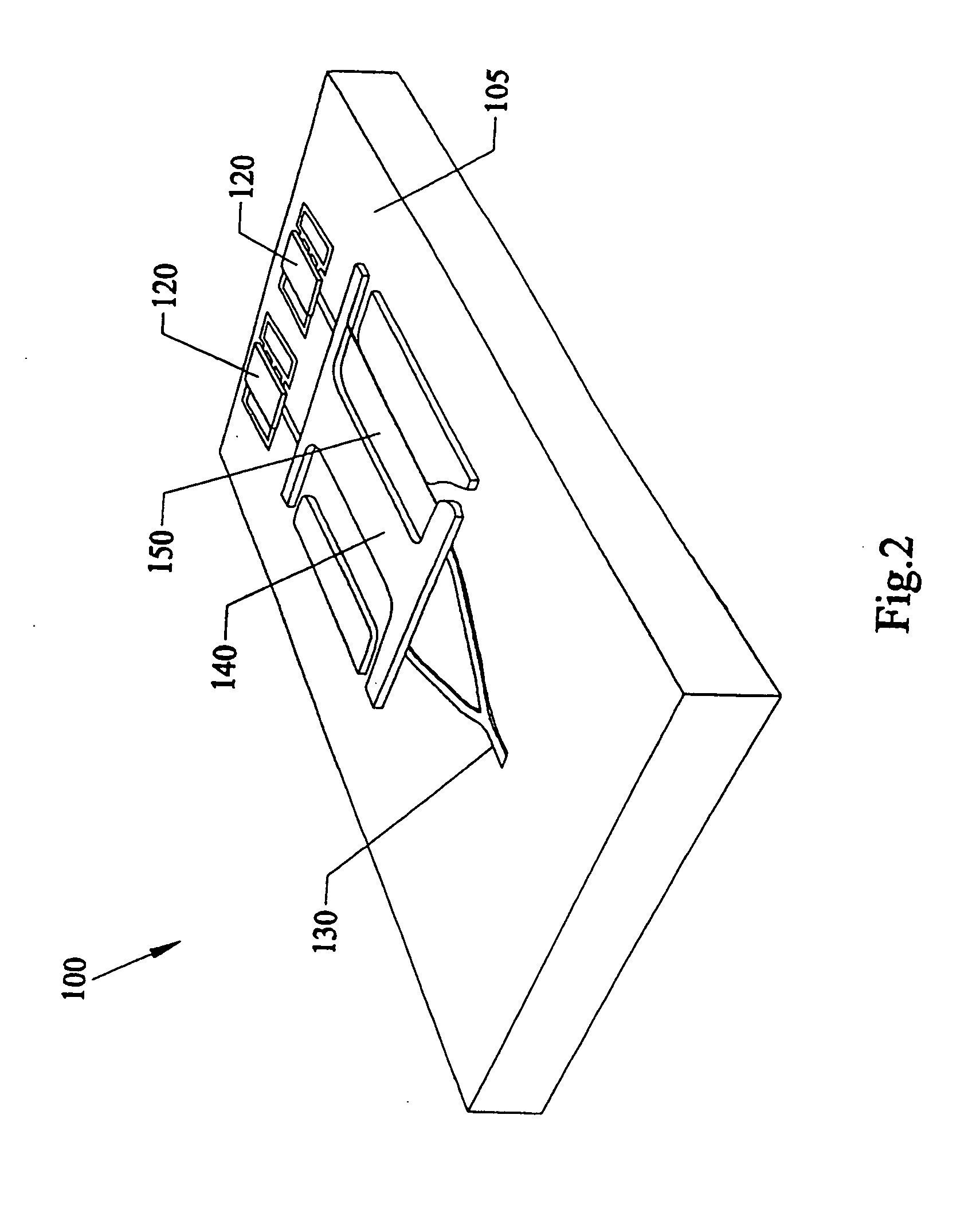
[0033]The following is a list of the reference numerals used in the drawings and the detailed specification to identify components. In the description of the preferred embodiments and the figures, like components are identified by like reference numerals.

10reflector type SPR sensor12polarized light14prism16reflected light18CCD array22metal film24fluidic sample26fluidic channel100planar integrated optical waveguide SPR sensor105substrate106SiON Layer107SiO2 layer110wavelength tunable laser120photodectors122poly silicon layer130optical waveguide133reference branch135sensing branch140micro-fluidic components142micromixer144micro-fluidic...


PUM

PropertyMeasurementUnit
refractive indexaaaaaaaaaa
wavelengthaaaaaaaaaa
wavelength tunableaaaaaaaaaa

Abstract

An integrated optical waveguide type surface plasmon resonance (SPR) sensor having an optical waveguide with a corresponding SPR sensing area, photodetectors, and wavelength tunable laser or any kind of external tunable laser source / coupler formed on a substrate. In an embodiment, the laser is a wavelength tunable laser and optionally, the integrated device may include a power source on the substrate for providing a electric power to the wavelength tunable laser and the photodetectors, or a circuit for signal processing, or a microfluidic structure for routing a target sample to the SPR sensor area. The microfluidic structure optionally includes a mixer or a reaction chamber for mixing and allowing a physical or chemical reaction to occur, respectively. In an embodiment, plural planar integrated optical waveguide type SPR sensors may be fabricated on a substrate to form an array of SPR sensors.

Description

[0001]This application claims the benefit of priority to U.S. Provisional Patent Application No. 60 / 635,725 filed on Dec. 10, 2004.FIELD OF THE INVENTION[0002]This invention relates to surface plasmon resonance sensors and, in particular, to methods, systems, apparatus and devices for integrating the optical waveguide, photodector, surface plasmon resonance (SPR) detection layer, and optionally included microfluidic structure on a single substrate to provide a micro integrated planar optical waveguide type surface plasmon resonance sensor.BACKGROUND AND PRIOR ART[0003]Basic working principle of surface plasmon resonance (SPR) sensor is inducing a spectrum of light into a sensing region and analyzing the absorption spectrum from the sensing region. Generally, inducing a spectrum of light on a sensing layer can be achieved in two ways; shining single wavelength of light with a range of incident angle or inducing a wavelength range of light. Sensor type is divided into two correspondin...

Claims


Application Information

Patent Timeline
Patent Type & Authority Applications(United States)
IPC IPC(8): G01N21/55
CPCG01N21/05G01N2021/0346G01N21/553
Inventor CHO, HYOUNG JINBANG, HYUNGSEOKWA, PATRICK LI KAM
Owner UNIV OF CENT FLORIDA RES FOUND INC
Why Eureka
Try Eureka