Structure and method for improving storage latch susceptibility to single event upsets

Inactive Publication Date: 2009-10-01
GLOBALFOUNDRIES INC
View PDF9 Cites 45 Cited by
  • Summary
  • Abstract
  • Description
  • Claims
  • Application Information

AI Technical Summary

Benefits of technology

[0009]In another embodiment, a static random access memory (SRAM) cell includes cross coupled first and second complementary metal oxide semiconductor (CMOS) inverters formed on a semiconductor substrate, the CMOS inverters including a first storage node and a second storage node that is the logical complement of the first storage node; a first access transistor coupled between the first storage node and a true data bit line, and a second access transistor coupled between the second storage node and a complement data bit line, the first and second access transistors activated by a word line coupled to gate conductors thereof; both of the first and second storage nodes each further selectively coupled to a deep trench capacitor through a switching transistor, with the switching transistors controlled by a common capacitance switch line coupled to gate conductors thereof; wherein, in a first mode of operation, the switching transistors are rendered nonconductive so as to isolate the deep trench capacitors from the inverter storage nodes and, in a second mode of operation, the switching transistors are rendered conductive so as to couple the deep trench capacitors to their respective stor

Problems solved by technology

In turn the operation of a circuit may be altered in such a way so as to cause an error in logic function, potentially crashing a computer system.
SEUs present significant reliability concerns in terrestrial and space environments.
Technology hardening is generally not commercially viable due to the expense associated with designing and improving existing fabrication methods, which can cost billions of dollars to develop in the first place.
Moreover, passive hardening is not efficient.
Although it is a workable solution, it repr

Method used


Image

  • Structure and method for improving storage latch susceptibility to single event upsets
  • Structure and method for improving storage latch susceptibility to single event upsets
  • Structure and method for improving storage latch susceptibility to single event upsets

Examples


Embodiment Construction

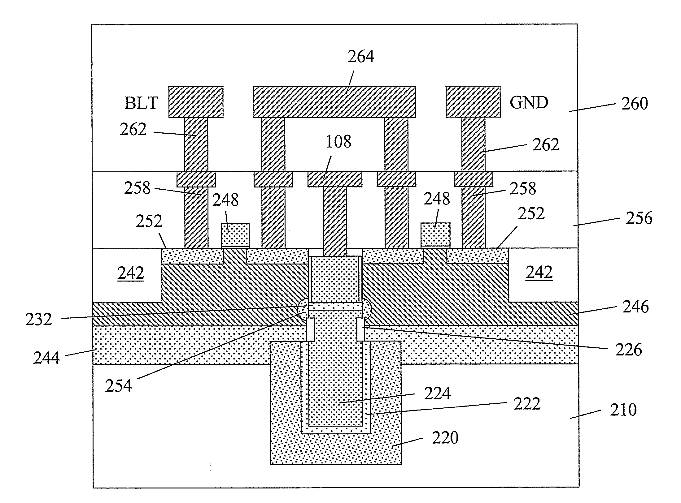
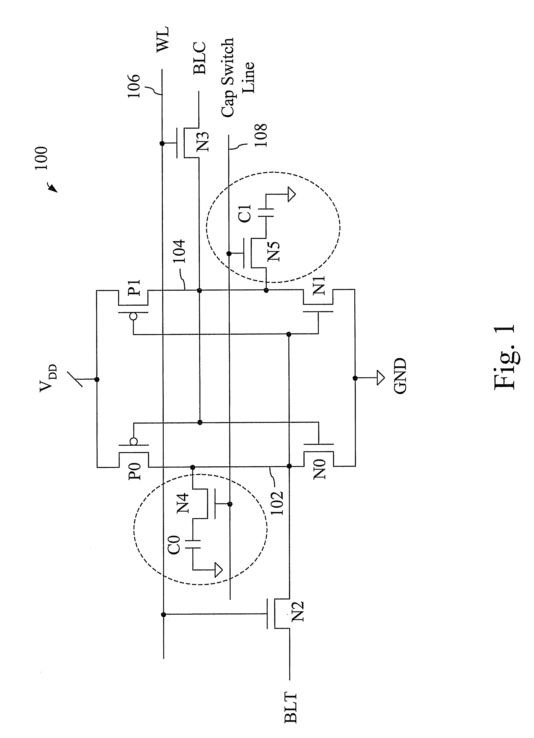
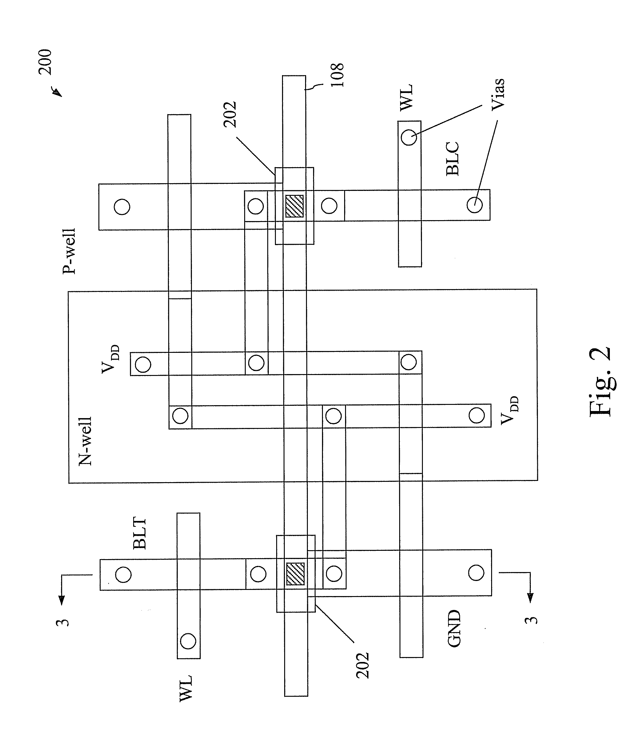
[0019]Disclosed herein is a structure and method for improving storage latch susceptibility to single event upsets (SEUs). Briefly stated, the invention embodiments presented herein provide an SEU hardened structure with added internal node capacitance in a manner that avoids sacrificing performance. Since the added capacitance can be selectively connected to or disconnected from the true and complement internal nodes of an SRAM cell, or a flip-flop in logic sequential circuits, by a switching MOSFET, the performance is improved over conventional approaches where the added capacitance is not selectively removable. This is especially true for a write operation, as the read operation is not effected by additional capacitance. During a write operation, the capacitors may be disconnected from the internal nodes, thus improving SEU immunity without sacrificing write performance.

[0020]Moreover, from a device area perspective, the added capacitance is realized through the formation of deep...


PUM


Abstract

A digital logic storage structure includes cross coupled first and second complementary metal oxide semiconductor (CMOS) inverters formed on a semiconductor substrate, the CMOS inverters including a first storage node and a second storage node that is the logical complement of the first storage node; both of the first and second storage nodes each selectively coupled to a deep trench capacitor through a switching transistor, with the switching transistors controlled by a common capacitance switch line coupled to gate conductors thereof; wherein, in a first mode of operation, the switching transistors are rendered nonconductive so as to isolate the deep trench capacitors from the inverter storage nodes and, in a second mode of operation, the switching transistors are rendered conductive so as to couple the deep trench capacitors to their respective storage nodes, thereby providing increased resistance of the storage nodes to single event upsets (SEUs).

Description

CROSS-REFERENCE TO RELATED APPLICATIONS[0001]This non-provisional U.S. patent application is co-pending with U.S. patent application Ser. No. 11 / 612,809, which was filed Dec. 19, 2006, and is assigned to the present assignee.BACKGROUND OF THE INVENTION[0002]The present invention relates generally to integrated circuit (IC) devices and, more particularly, to structure and method for improving storage latch susceptibility to single event upsets (SEUs).[0003]The effects of radiation on integrated circuits have been known for many years. These effects may be broken down into two broad categories, namely “total dose effects,” in which an integrated circuit gradually deteriorates due to the accumulated effect of all the damage done to the crystal structure by the many particles incident thereupon, and “single event effects” in which a single particle (either through its exceptionally high energy or through the accuracy of its trajectory through a semiconductor) is capable of affecting a c...

Claims


Application Information

Patent Timeline
IPC IPC(8): G11C11/40H01L21/8244H01L27/11
CPCG11C11/4125H01L27/0921H03K3/0375H01L27/1104H01L29/66181H01L27/11H10B10/00H10B10/12
Inventor CANNON, ETHAN H.FURUKAWA, TOSHIHARUHORAK, DAVIDKOBURGER, III, CHARLES W.MANDELMAN, JACK A.
Owner GLOBALFOUNDRIES INC
Why Eureka
Try Eureka