PLL circuit

a phaselocked loop and circuit technology, applied in the field of pll (phaselocked loop) circuits, can solve the problems that the technology of the past cannot deal with such changes

Inactive Publication Date: 2009-10-01
SONY CORP
View PDF3 Cites 7 Cited by
  • Summary
  • Abstract
  • Description
  • Claims
  • Application Information

AI Technical Summary

Benefits of technology

[0015]In view of the above, the present invention is to improve the characteristic of the PLL circuit and simplify configuration therefor.
[0017]According to the present invention, the PLL characteristic of a PLL circuit that needs to have a wide frequency range can be held constant, and a configuration therefor is simple.

Problems solved by technology

However, technology in the past cannot deal with such changes in the band WC.

Method used


Image

  • PLL circuit
  • PLL circuit
  • PLL circuit

Examples


embodiment

[2] Embodiment

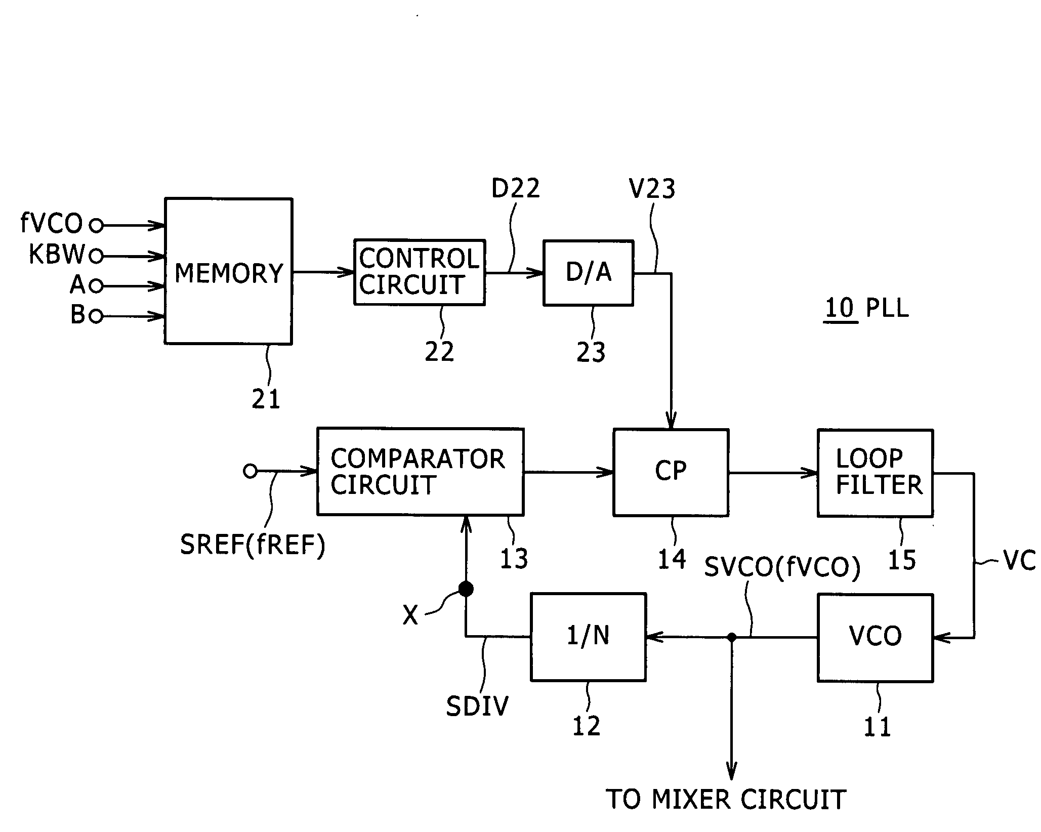
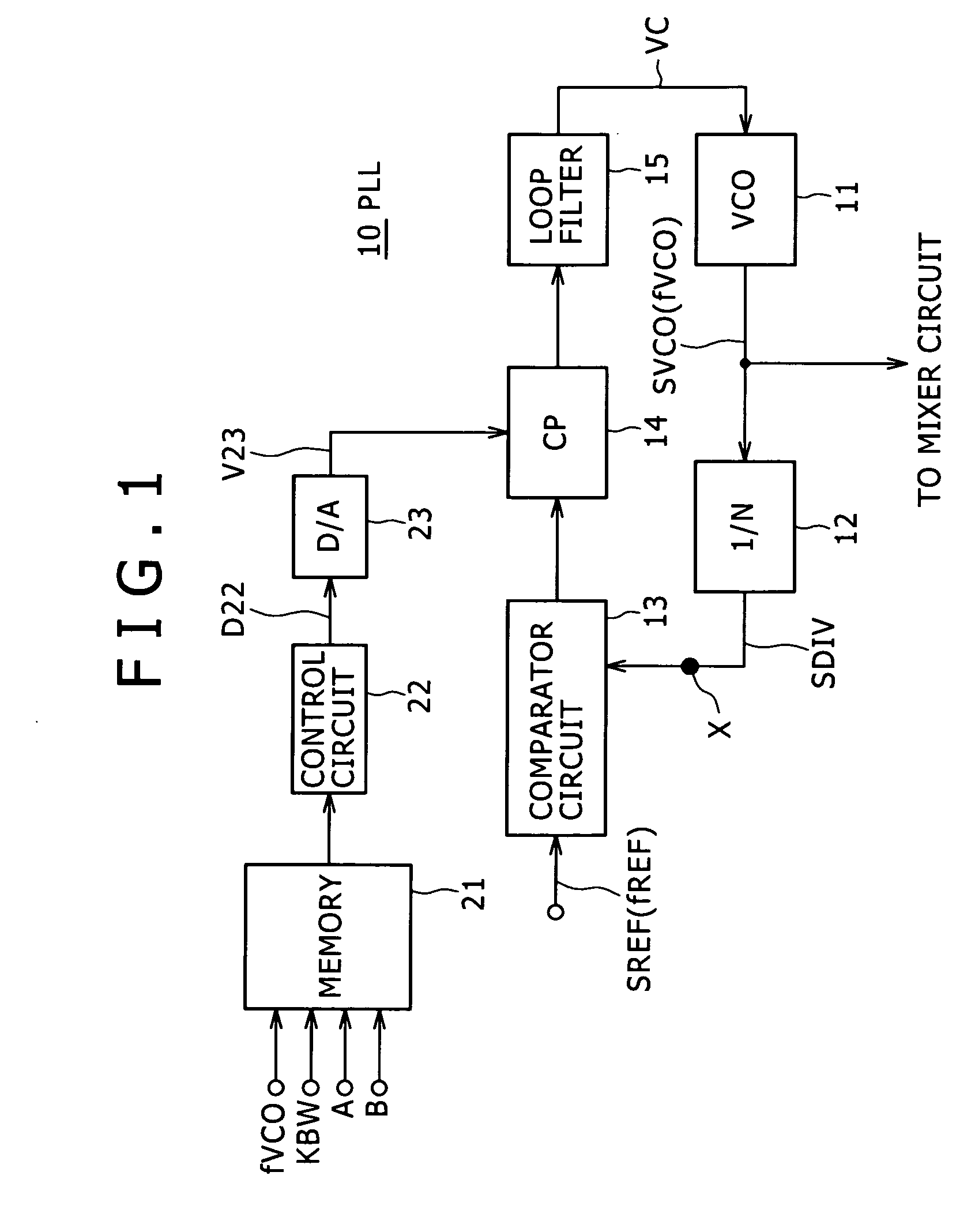
[0047]As described in [1-1], the basic PLL circuit is formed as indicated by reference numeral 10 in FIG. 1, for example, and is integrated into one IC on a chip together with the circuits 21 to 23.

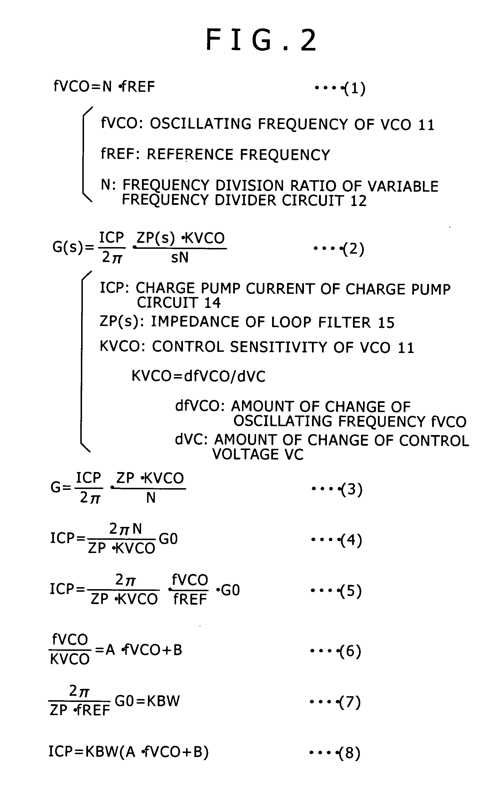
[0048]Further, in FIG. 1, data indicating the oscillating frequency fVCO of the VCO 11, data on the constant KBW determining the band WC, and data on the constants A and B determining the control sensitivity KVCO of the VCO 11 are prepared. These pieces of data are stored in the memory (register) 21, and supplied to the control circuit 22 to be converted into data D22 corresponding to the data described in [1-3].

[0049]The data D22 is supplied to the D / A converter circuit 23 to be converted into an analog voltage V23 by D / A conversion, the voltage V23 is supplied to constant-current sources Q1 and Q2 as a control voltage for controlling the charge pump current ICP (output current), and the magnitude of the charge pump current ICP is controlled as described in [1-3].

[0050]Inci...


PUM


Abstract

Disclosed herein is a phase-locked loop circuit including: a voltage controlled oscillator; a variable frequency divider circuit for frequency-dividing an oscillating signal of the voltage controlled oscillator into a 1 / N (N is an integer) frequency; a phase comparator circuit for comparing phases of a frequency-divided signal and a reference signal of a reference frequency with each other; a charge pump circuit for outputting a charge pump current changed in pulse width; a loop filter for being supplied with the charge pump current and outputting a direct-current voltage changed in level; and a control circuit for calculating a value of the charge pump current as a function of the oscillating frequency of the voltage controlled oscillator and a coefficient for setting a phase locked loop band, and setting the value of the charge pump current in the charge pump circuit.

Description

BACKGROUND OF THE INVENTION[0001]1. Field of the Invention[0002]The present invention relates to a PLL (phase-locked loop) circuit.[0003]2. Description of the Related Art[0004]When a superheterodyne receiver is configured into a synthesizer system, the local oscillating signal of the receiver is formed by a PLL circuit. The PLL circuit is generally formed as indicated by reference numeral 10 in FIG. 6. Specifically, in the PLL circuit 10, an oscillating signal SVCO of a VCO (voltage controlled oscillator) 11 is supplied to a variable frequency divider circuit 12 to be frequency-divided into a frequency-divided signal SDIV of a 1 / N (N is a positive integer) frequency. The frequency-divided signal SDIV is supplied to a phase comparator circuit 13. In addition, a reference signal SREF of a frequency fREF serving as a reference is supplied to the phase comparator circuit 13.[0005]The phase comparator circuit 13 compares the phases of the frequency-divided signal SDIV and the reference s...

Claims


Application Information

Patent Timeline
Patent Type & Authority Applications(United States)
IPC IPC(8): H03D3/24
CPCH03L7/0896H03L7/183H03L7/093H03L7/0898
Inventor MIURA, KIYOSHIMIURA, MICHIKO
Owner SONY CORP
Why Eureka
Try Eureka