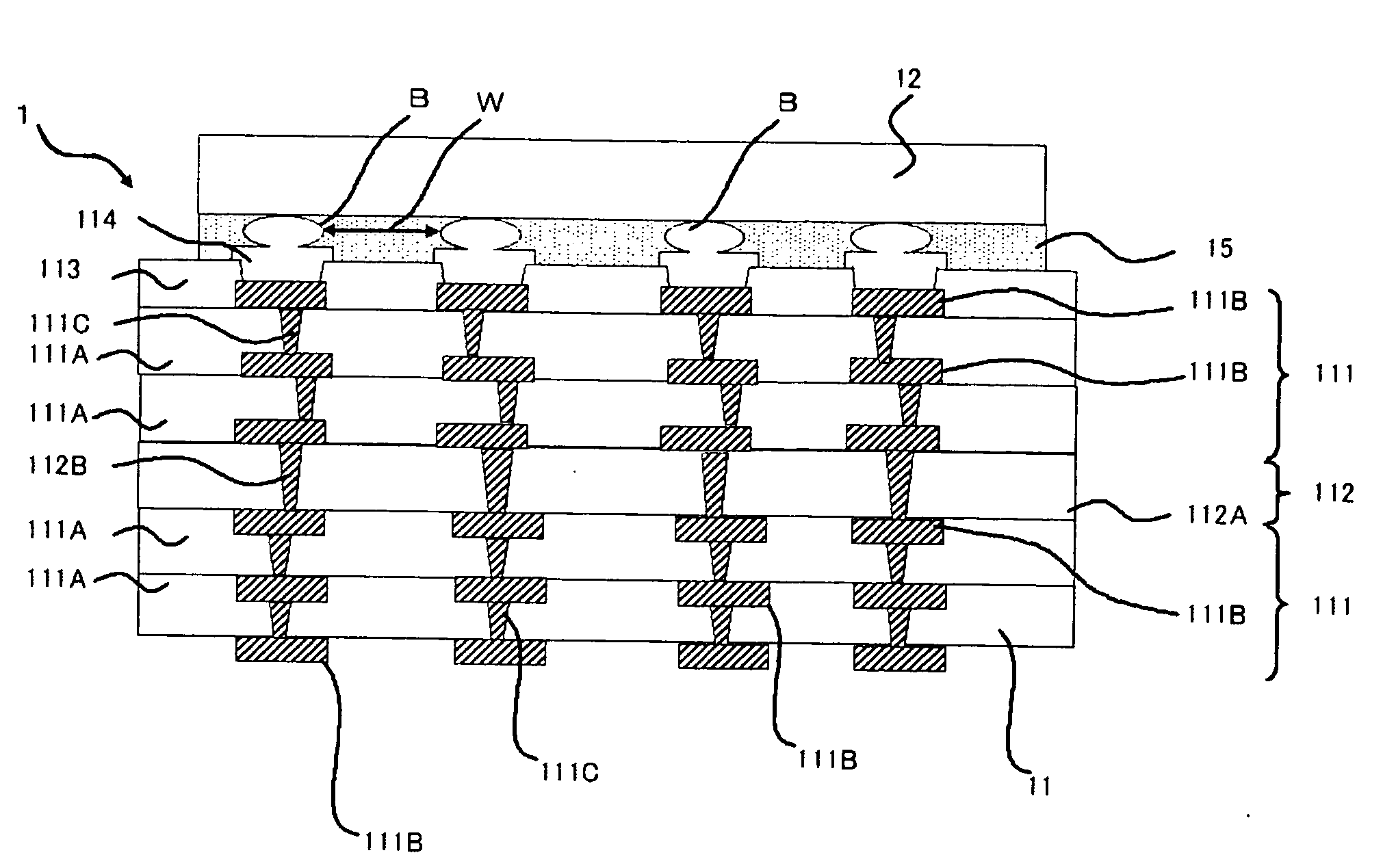
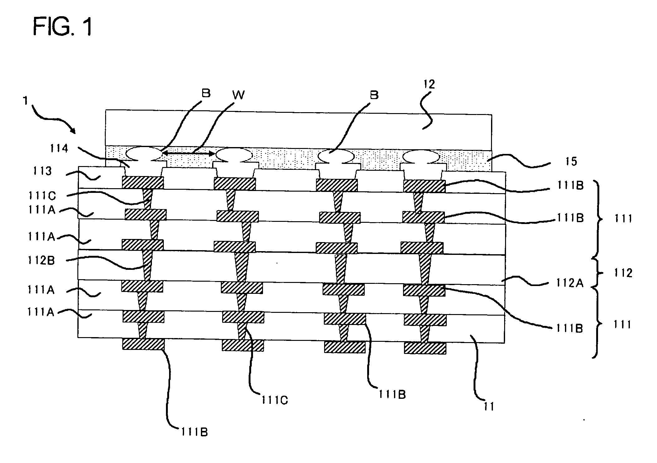
[0048]Next, advantageous effects of the present embodiment will be described. In the present embodiment, the resin 15 is supplied to the spaces or the gaps surrounded by the semiconductor element 12, the resin substrate 11 and the bumps B under the condition that the water content of the resin substrate 11 is equal to or lower than 0.02% and the resin 15 is cured. This ensures inhibiting a generation of voids in the resin 15. This allows preventing a quality deterioration of the manufactured
semiconductor device 1. In particular, in the present embodiment, the distance between the solder bumps B is provides as equal to or smaller than 200 μm. When the solder bumps B are arranged with such narrower inter-bump distances, a void in the resin 15 may cause unwanted coupling between the solder bumps B. A generation of such voids may cause the melted solder bump B and the melted solder section 114 entering into the voids, leading to creating an electrical coupling between the solder bumps B fellow, thereby possibly cause a short-circuit. Since the solder bumps B and the solder sections 114 are composed of lead-free solder in the present embodiment, the solder bumps B and / or the solder sections 114 may be melted when the semiconductor device 1 is installed onto a mother board to cause a penetration of such melted material in the voids. On the contrary, since the generation of voids in the resin 15 can be inhibited according to the process in the present embodiment, deterioration in the quality of the semiconductor device 1 can be prevented.
[0049]In the conventional semiconductor device, lead-containing solder is often employed for the bumps for coupling the semiconductor element with the resin substrate. Therefore, even if the semiconductor device is heated in the process for installing the semiconductor device onto the mother board, the bumps are not melted, and thus short circuits resulted from the coupling of the bumps are scarcely caused. In addition, the distance between the bumps that couple the semiconductor element with the resin substrate is relatively larger in the conventional semiconductor device (for example, about 250 μm). Therefore, even if smaller voids are generated in the underfill, the voids do not connect the bumps. Therefore, even if the bumps are melted, it scarcely happens that the bumps are connected to cause a short-circuit. On the contrary, in the semiconductor device 1 of the present embodiment, the distances between the solder bumps B are selected to be equal to or lower than 200 μm and lead-free solder is employed for the bumps B and the solder section 114, as described above. Therefore, the
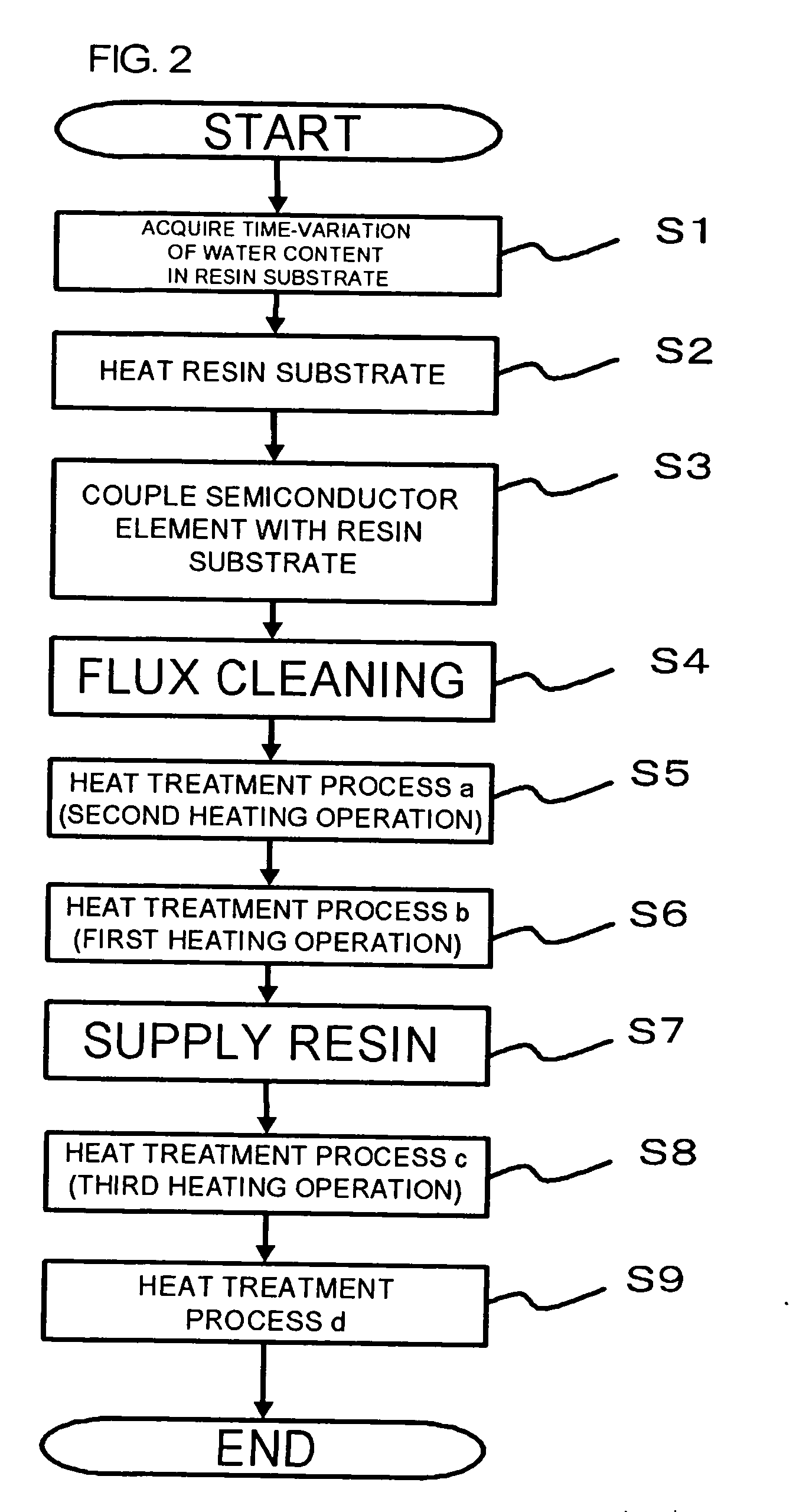
heating time and the storage time should be strictly managed to avoid a generation of even relatively smaller voids. Thus, in the present embodiment, the time-variation of the water content in the resin substrate 11 is previously determined, and the time elapsed from the end of the heating operation for
outgassing from the resin substrate 11 (processing S5) to the start of the heating operation for providing the water content of the resin substrate 11 of equal to or lower than 0.02% (processing S6) is determined. Then, the water content of the resin substrate 11 right before the heating operation for providing the water content of the resin substrate 11 of equal to or lower than 0.02% is determined on the basis of the determined time and the data of the time-variation of the water content in the resin substrate 11, and the heating process is carried out on the basis of the determined water content to achieve the controlled water content of the resin substrate 11 as equal to or lower than 0.02%. This ensures the water content of the resin substrate 11 to be equal to or lower than 0.02%, so that the prevention for generation the voids in the resin 15 is strictly managed.
[0050]On the other hands, Japanese Patent Laid-Open No. 2002-313,841 describes that a
sealant is supplied after the substrate is dried, and then the
semiconductor chip is compressively adhered thereto and the
sealant is cured. It is also disclosed that the supply of the
sealant should be carried out over a short period of time in such process, in order to hold the temperature of the substrate at a
drying temperature from the compressive
bonding process of the
semiconductor chip and the curing process of the sealant. In such type of process, a series of operations from
drying the substrate to supplying the sealant should be rapidly carried out, and thus, if a plurality of substrates are to be dried, it is difficult to carry out the supply of the sealant while holding all the substrates at the
drying temperature. In addition, while Japanese Patent Laid-Open No. 2002-313,841 also describes that the substrate is heated again to carry out the compressive bonding of the the
semiconductor chip and the cure of the sealant if the temperature of the substrate is decreased due to the standing still after drying the substrate, such increase of the temperature of the substrate to the drying temperature does not necessarily achieve the sufficient removal of water in the substrate. Therefore, a generation of voids due to water in the substrate in may be caused in the sealant. On the contrary, it is found in the present embodiment that voids are easily generated in the resin 15 when the water content in the resin substrate 11 is beyond 0.02%, and the time-variation of the water content in the resin substrate 11 is determined. Therefore, even if a number of semiconductor devices are treated in the
heat processing operation S5 and the processed semiconductor devices are stored in a predetermined location, the water content in the resin substrate 11 can be calculated based on the storage time and the time-variation of the water content of the resin substrate 11. Then, a heat-processing is conducted in the
heat processing operation S6 according to the calculated water content to control the water content of the resin substrate 11 to be equal to or lower than 0.02%, and then the resin is supplied while maintaining such condition to ensure preventing a generation of voids.
[0051]Further, many of the underfill resins that are currently employed are cured at a temperature of equal to or higher than 100 degree C. Therefore, in the process described in Japanese Patent Laid-Open No. 2004-260,096, it is difficult to obtain sufficiently increased
viscosity of the underfill resin in the first heating operation of Japanese Patent Laid-Open No. 2004-260,096. Therefore, it is difficult to firmly prevent a generation of voids. In addition, a need for employing a special resin, which provides an increased
viscosity of the underfill resin under the condition employed in the first heating operation disclosed in Japanese Patent Laid-Open No. 2004-260,096, is caused, leading to a problem of being unable to employ a
general purpose underfill resin. On the contrary, since the resin 15 is supplied under the condition for providing the water content of the resin substrate 11 to be equal to or lower than 0.02% in the present embodiment, a generation of void can be firmly inhibited, and a need for employing a resin having a special composition for the resin 15 is eliminated.
[0052]Further, in general, in order to carry out the seal with the resin within a short period of time, it is necessary to provide a
reduced viscosity of the underfill resin when the spaces between the bumps are filled with the underfill resin. It is general to utilize a heating process as a manner for providing a
reduced viscosity of the underfill resin. A use of a type of resin, which exhibits an increased viscosity when the resin is heated to a temperature below the
boiling point lower of water, is required in the process described in Japanese Patent Laid-Open No. 2004-260,096. When such underfill resin is injected to the spaces between the bumps, the reduction of the viscosity of the resin should be achieved by heating the resin to a temperature, which is lower than the above-described temperature for obtaining the increase of the viscosity. In this case, it is presumed that an appropriate viscosity of the resin cannot be obtained for suitably supplying the underfill resin via a capillary phenomenon. Further, even if the supply of the underfill resin can be conducted, it is also presumed that longer period of time is required until the completion of the resin seal. On the contrary, a use of a special resin, which exhibits an increased viscosity at a temperature below the
boiling point of water, is not required in the present embodiment, and a general underfill resin may be employed, so that a rapid supply of the underfill resin can be achieved.
[0053]The present invention is not limited to the above-mentioned embodiments, and a modification or an improvement within the range for achieving the purpose of the present invention are also included in the present invention. For example, while the build-up substrate having the core layer 112 and the build-up layer 111 is employed for the resin substrate 11 in the above-described embodiments, the resin substrate 11 is not limited thereto, and a build-up substrate having no core layer may also be employed.

