

Organic electroluminescent element manufacturing method
- Summary
- Abstract
- Description
- Claims
- Application Information
AI Technical Summary
Benefits of technology
Problems solved by technology
Method used
Image

Examples
first preferred embodiment
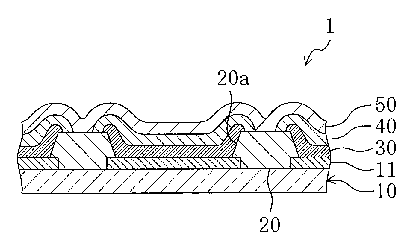
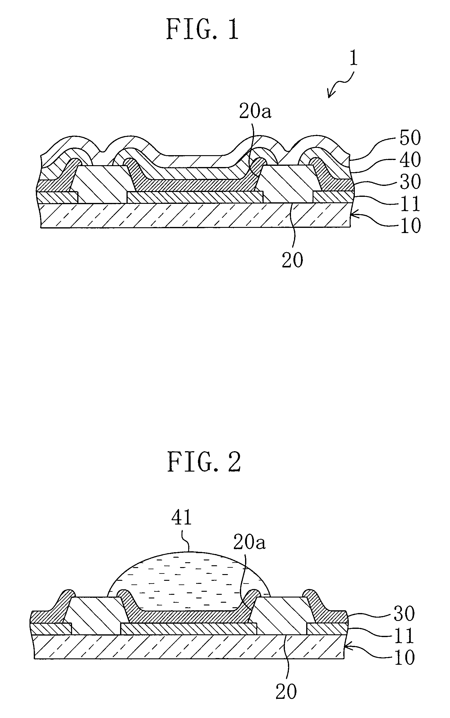
[0023]FIG. 1 is a sectional view of a portion of an organic EL element 1 in accordance with the first preferred embodiment.
[0024]First, a structure of the organic EL element 1 manufactured according to the first preferred embodiment will be described with reference to FIG. 1. The organic EL element 1 preferably includes an active matrix substrate 10 having a surface on which a plurality of first electrodes (anodes) 11 are arranged in matrix, a bank (diaphragm) 20; a buffer layer 30, a light emitting layer 40, and a second electrode 50 (cathode). The bank 20 is formed on the active matrix substrate 10. In the bank 20, a plurality of openings 20a preferably having a circular or substantially circular shape in a plan view are formed through which the plurality of first electrodes 11 formed on the active matrix substrate 10 are exposed. In the first preferred embodiment, the bank 20 preferably has a substantially trapezoidal shape in transverse section. The “substantially trapezoidal sh...
modified example
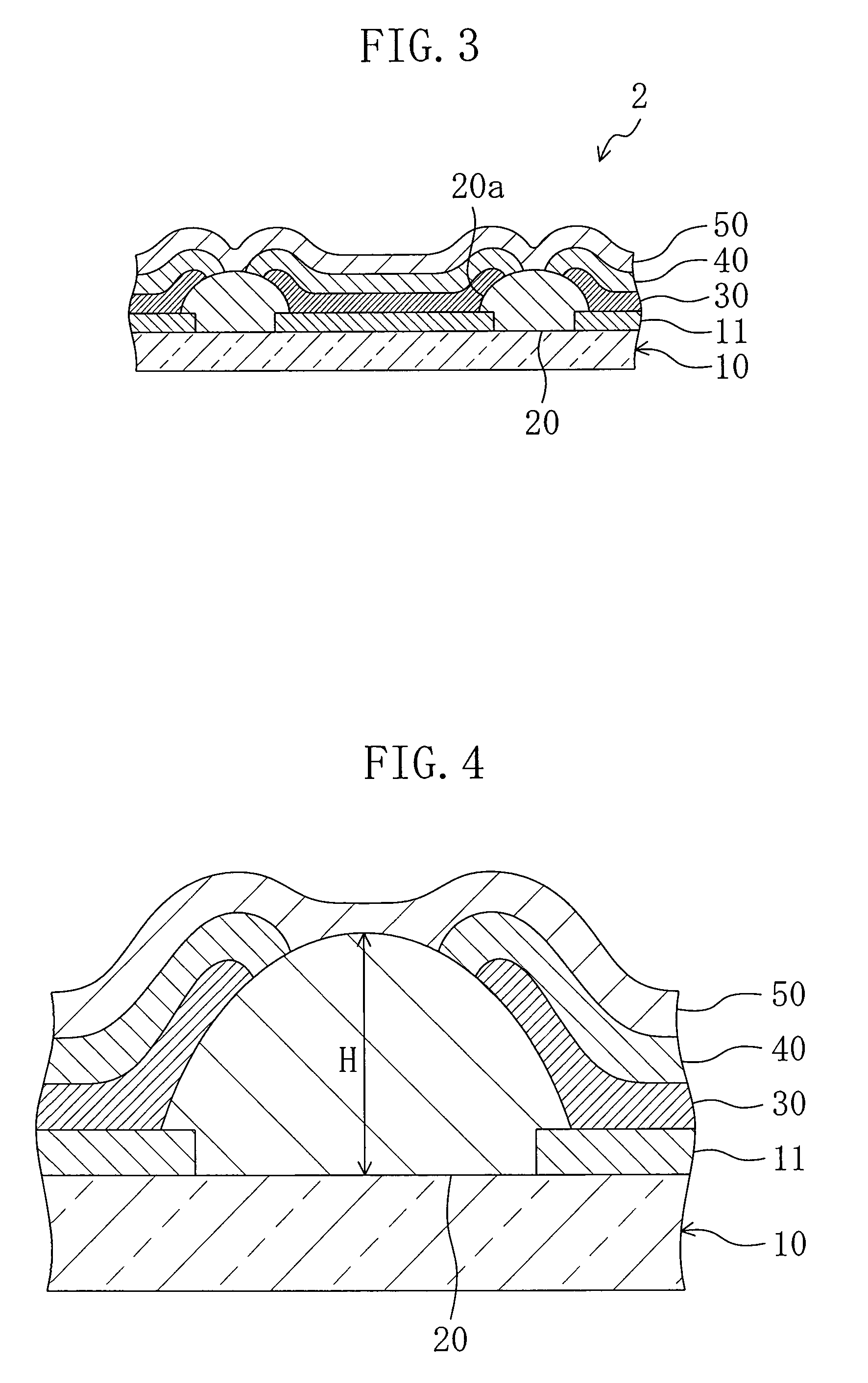
[0042]FIG. 3 is a sectional view of a part of an organic EL element 2 in accordance with modified example of a preferred embodiment of the present invention.
[0043]FIG. 4 is an enlarged sectional view of the vicinity of a bank 20 of the organic EL element 2.
[0044]Though the first preferred embodiment refers to manufacture of the organic EL element 1 in which the bank 20 preferably having a substantially trapezoidal shape in transverse section is formed, the shape of the bank 20 is not limited in the present invention. For example, as in the present modified example, the bank 20 may have a dome-like shape in transverse section (to have a curved surface).
[0045]In the case where the bank 20 has a dome-like shape in transverse section as in the present modified example, the buffer layer 30 preferably covers a lower part of the bank 20 of which height is H / 2 or larger (preferably, 3H / 5 or larger, and more preferably, 7H / 10 or larger) where H is the height from the active matrix substrate ...
example 1
[0046]The same organic EL element as in the first preferred embodiment was manufactured for Example 1.
[0047]First, an active matrix substrate 10 having a surface on which first electrodes 11 made of indium tin oxide (ITO) are arranged in matrix was prepared. An acryl resin film was formed by spin coating a photosensitive acryl resin onto the active matrix substrate 10. The thus formed acryl resin film was patterned by photolithography to form a bank 20. Openings 20a formed in the bank 20 were substantially circular having a radius of about 200 μm.
[0048]Next, the thus formed bank 20 and the first electrodes 11 were subjected to a plasma treatment using an oxygen gas and a fluorocarbon gas to provide a repellent property to the surface of the bank 20 and to provide a lyophilic property to the surface of each first electrode 11.
[0049]Subsequently, an ink for forming a hole transport layer (a hole transport layer forming ink) is prepared by using an aqueous dispersion of poly(3,4-ethyle...
PUM
 Abstract
Description
Claims
Application Information