Film thickness measuring apparatus and film thickness measuring method

a technology of measuring apparatus and film thickness, which is applied in the direction of electrical/magnetic thickness measurement, material magnetic variables, instruments, etc., can solve the problems of wiring insulation failure, frequency shift variation, and work for it becoming unnecessary

Inactive Publication Date: 2009-10-15
TOKYO SEIMITSU
View PDF7 Cites 35 Cited by
  • Summary
  • Abstract
  • Description
  • Claims
  • Application Information

AI Technical Summary

Benefits of technology

[0036]The present invention is proposed in order to attain the above-mentioned object, and the invention according to claim 1 provide a film thickness measuring method which, in a film thickness measuring method for measuring a film thickness of a conductive film formed on a substrate, opposes a coil to a surface of a conductive film, makes a magnetic field induced in the coil by an alternating current supplied to the coil operate on the conductive film, forms a ...

Problems solved by technology

If polishing of the conductive film is excessive, the resistance of the wiring increases, and if polishing of the conductive film is too little, it leads to an insulating failure of the wiring.
Second, when the thickness of the conductive film decreases, the effect as if the metal rod is drawn out from the coil of the inductor will arise therein, and this will cause a variation of the inductance and the frequency shift.
First, by using photo lithography and forming with a thin film on the same substrate, relative position accuracy of a coil and a displacement sensor is improved by leaps and bounds, and a jig for adjusting a relative position and work for it becomes unnecessary.
However, although the magnetic leakage flux induces the eddy current, which becomes Joule's heat to be consumed in the form of the eddy current loss after all.
However, in the inner part wired thereon already, since a wiring cross section is small and the volume resistivity is small, a large eddy current is induced by penetrating magnetic flux, and as a result, large joule thermal loss will be induced locally.
This problem sometimes develops into the melting and breaking of the wiring in a part.
Further, for example, in the case of performing process by changing a polishing condition, at the time point when the amount of residual films reached at the predetermined value around the polishing end time point, it is difficult to discern whether the amount of residual films is the predetermined amount.
Accordingly, even if the setting which discriminates the polishing end point is per...

Method used


Image

  • Film thickness measuring apparatus and film thickness measuring method
  • Film thickness measuring apparatus and film thickness measuring method
  • Film thickness measuring apparatus and film thickness measuring method

Examples


Embodiment Construction

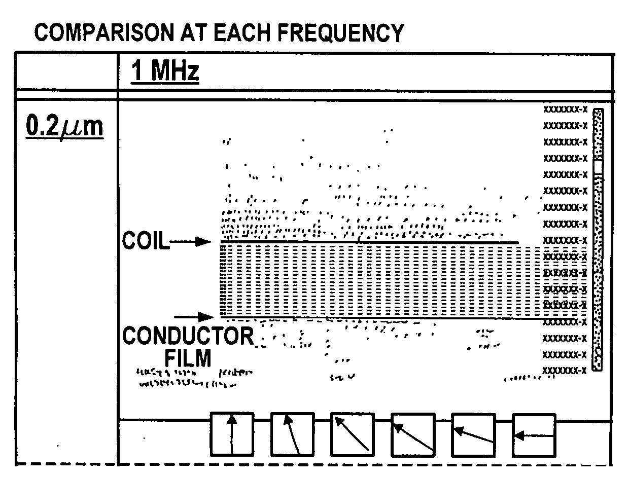
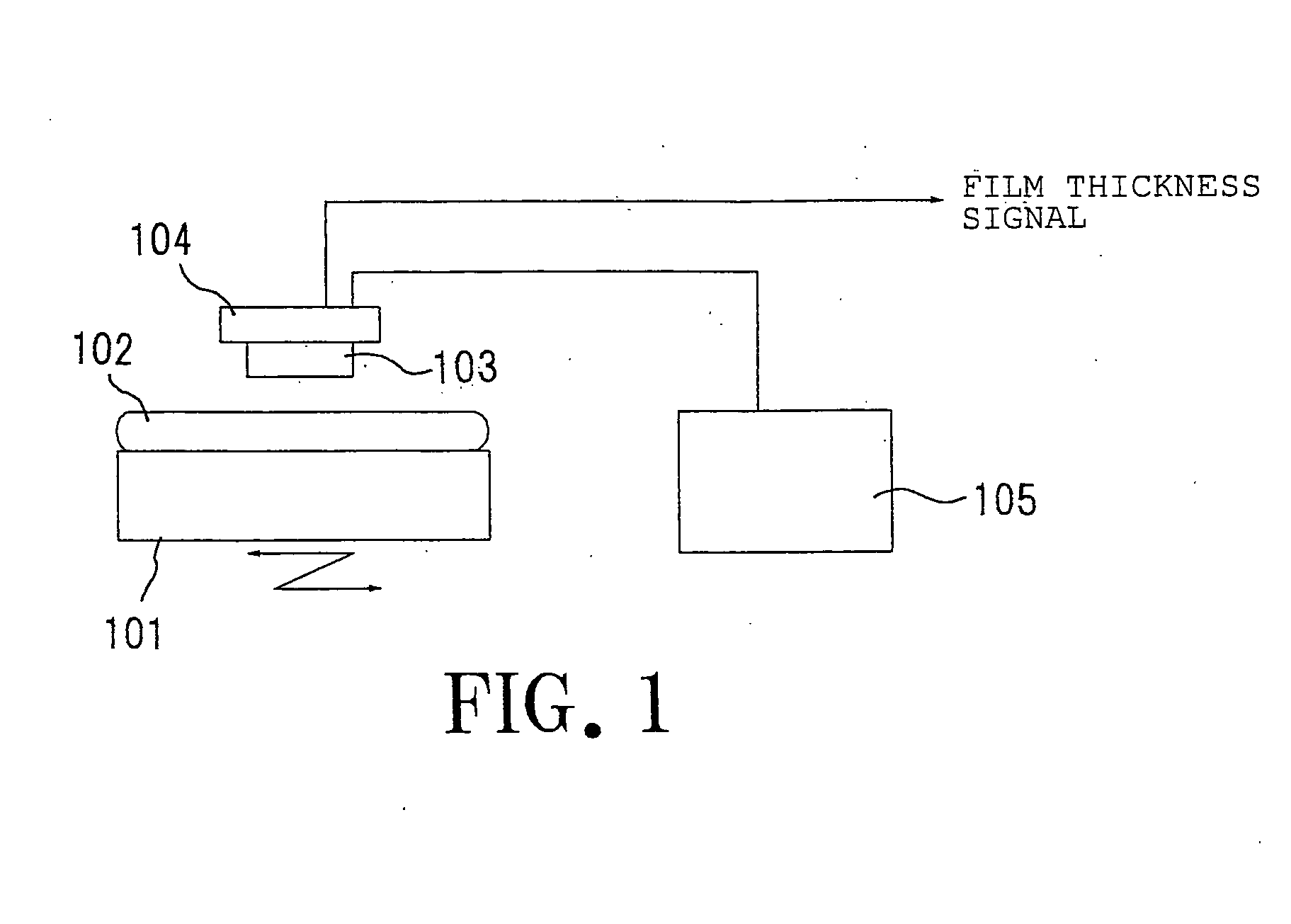
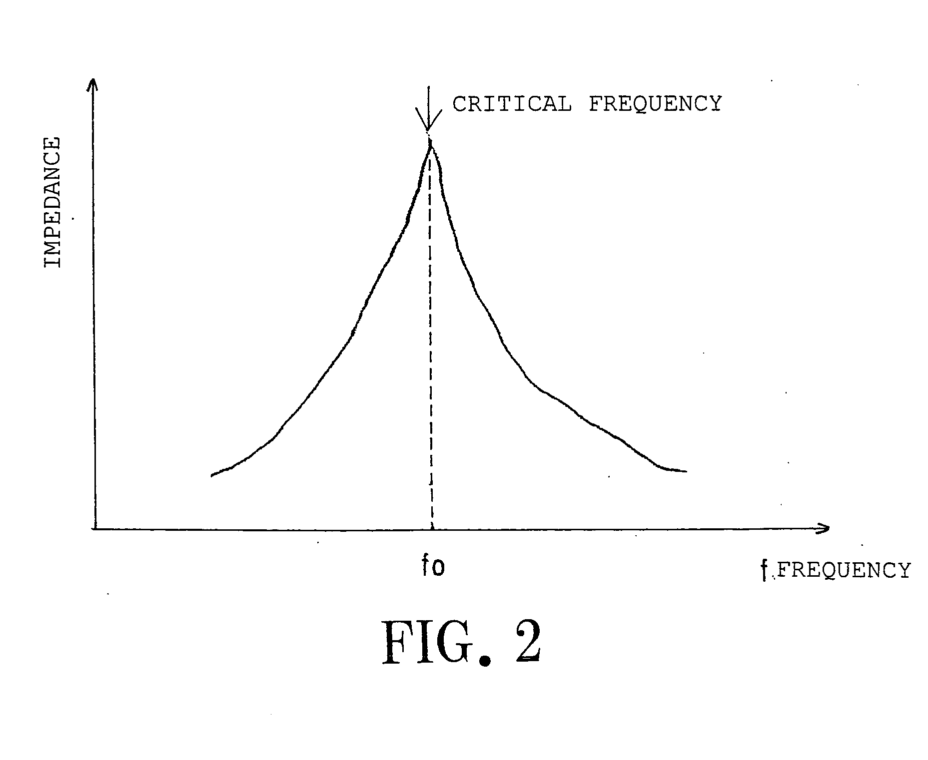
[0095]The present invention has been realized by providing the film thickness measuring method and the apparatus characterized in that, in the film thickness measuring method measuring the film thickness of the conductive film formed on the substrate, in order to attain the object of the polishing end time point of the wafer being estimated and detected accurately, and of the amount of the residual film to be removed as well as the polishing rate, etc. being computed accurately in real time, and of the desired film thickness being made to be formed with a predetermined conductive film removed properly, by means of opposing the coil to the surface of the conductive film, making the magnetic field made to be induced by the coil with the alternating current supplied to the coil operate on the conductive film, and making parameters which influence the skin effect of the conductive film change and giving the parameters to the coil, the state of the magnetic field being made not to penetr...


PUM


Abstract

Coil is made to be disposed with gap opposed to the surface of wafer, and wafer stage is made to move in X and Y direction and R and θ direction. When supplying an alternating current to coil with the frequency swept by impedance analyzer, the magnetic field made to be induced in coil will operate on the conductive film of wafer. By changing a parameter (a frequency or an angle) influencing the skin effect of the conductive film and giving the parameter to coil, the state where a magnetic field is not made to penetrate relatively the film of wafer and the state where the magnetic field is made to penetrate relatively the film can be formed. From the variation of various values corresponding to the eddy current induced based on the change of state influenced by the skin effect of the conductive film, the film thickness of wafer can be measured with sufficient accuracy.

Description

BACKGROUND OF THE INVENTION[0001]1. Field of the Invention[0002]The present invention relates to a film thickness measuring apparatus and a film thickness measuring method which measure a film thickness of a polishing completion time point, and in particular, the present invention relates to the film thickness measuring apparatus and the film thickness measuring method which measures the film thickness of the polishing completion time point accurately without extending a strong magnetic flux against an element etc. formed on a device wafer after restraining joule thermal loss caused by an eddy current to the local minimum in a chemical mechanical polishing (CMP), etc.[0003]2. Description of Related Art[0004]Known is the process for forming a wiring pattern, where an oxide film is formed on a surface of a semiconductor wafer, and lithography and etching to this oxide film is performed, and a groove pattern corresponding to a wiring pattern is formed, and a conductive film which compr...

Claims


Application Information

Patent Timeline
IPC IPC(8): G01B7/06
CPCG01B7/105
Inventor FUJITA, TAKASHIYOKOYAMA, TOSHIYUKIKITADE, KEITA
Owner TOKYO SEIMITSU
Why Eureka
Try Eureka