Printed circuit board and method of manufacturing the same

a technology of printed circuit board and printed circuit, which is applied in the direction of printed circuit aspects, resist details, electric connection formation of printed elements, etc., can solve the problems of increasing the number of small circuits, increasing the number of circuits, and 3/b> having such a shape, and achieve high-density circuit patterns

Inactive Publication Date: 2009-10-22
SAMSUNG ELECTRO MECHANICS CO LTD
View PDF3 Cites 13 Cited by
  • Summary
  • Abstract
  • Description
  • Claims
  • Application Information

AI Technical Summary

Benefits of technology

[0012]In addition, the present invention provides a PCB and a method of manufacturing the same, in which the line width of a circuit pattern, which is connected to the upper portion of a via, is formed to be smaller than the diameter of the via, thus realizing a high-density circuit pattern.

Problems solved by technology

However, recently, as circuits become increasingly complicated and the demand for high-density and small circuits is increasing, double-sided PCBs or MLBs are mainly used.
The via hole 3 having such a shape is disadvantageous because it has physical properties inferior to those of a via hole having a constant diameter.
Due to the presence of the land 5, it is difficult to increase the density of the circuit pattern near the via.
Furthermore, the conductive paste prepared by mixing metal powder with resin material is dissatisfactory because its electrical signal transfer performance is inferior to that of metal.

Method used


Image

  • Printed circuit board and method of manufacturing the same
  • Printed circuit board and method of manufacturing the same
  • Printed circuit board and method of manufacturing the same

Examples


Embodiment Construction

[0026]Hereinafter, a detailed description will be given of a PCB and a method of manufacturing the same according to the present invention, with reference to the appended drawings. Throughout the drawings, like reference numerals refer to like elements, and redundant descriptions are omitted. In the description, the terms “first”, “second” and so on are used to distinguish one element from another element, but are not to be construed to limit the elements. Further, the terms and words used in the present specification and claims should not be interpreted as being limited to typical meanings or dictionary definitions, but should be interpreted as having meanings and concepts relevant to the technical scope of the present invention based on the rule according to which an inventor can appropriately define the concept of the term to describe the best method he or she knows for carrying out the invention.

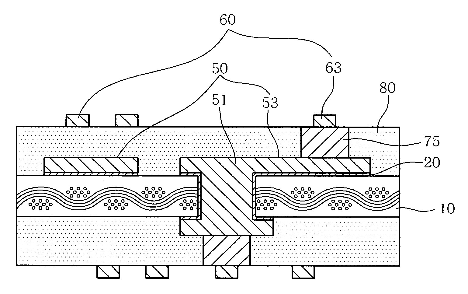
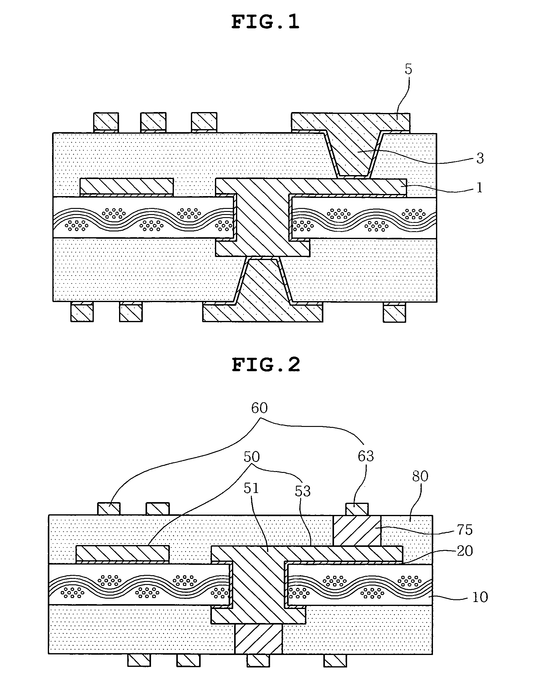
[0027]FIG. 2 is a cross-sectional view illustrating the PCB according to the present...


PUM

PropertyMeasurementUnit
thicknessaaaaaaaaaa
thickaaaaaaaaaa
thickness d1aaaaaaaaaa

Abstract

The printed circuit board includes the via formed with the electroplating layer unlike a conventional via formed with an electroless plating layer and an electroplating layer and having a cylindrical shape, and thus exhibits good interlayer electrical connection and high reliability of physical contact upon thermal stress caused by the variance in physical properties of material depending on changes in temperature. The via has no upper land, and thus a fine circuit pattern of the circuit layer can be formed on the via.

Description

CROSS REFERENCE TO RELATED APPLICATION[0001]This application claims the benefit of Korean Patent Application No. 10-2008-0036182, filed Apr. 18, 2008, entitled “Printed circuit board and method for manufacturing the same”, which is hereby incorporated by reference in its entirety into this application.BACKGROUND OF THE INVENTION[0002]1. Field of the Invention[0003]The present invention relates to a printed circuit board (PCB) and a method of manufacturing the same, and more particularly, to a PCB, which includes a via formed with an electroplating layer, without an electroless plating layer, thus realizing interlayer connection.[0004]2. Description of the Related Art[0005]Generally, a PCB is manufactured by attaching a thin film made of copper or the like to either surface of an insulating plate made of phenol resin or epoxy resin, etching the insulating plate with the thin film according to a wiring pattern of a circuit (such that portions other than the linear circuit are eliminat...

Claims


Application Information

Patent Timeline
Patent Type & Authority Applications(United States)
IPC IPC(8): H05K1/00H05K3/42
CPCH05K3/108H05K3/423H05K3/426H05K3/4647Y10T29/49165H05K2201/09545H05K2203/0574H05K2203/0733H05K2201/09536H05K1/11
Inventor OH, CHANG GUNHWANG, MI SUNLEE, SUK WON
Owner SAMSUNG ELECTRO MECHANICS CO LTD
Why Eureka
Try Eureka