Applying trenched transient voltage suppressor (TVS) technology for distributed low pass filters

a low-pass filter and transient voltage suppressor technology, applied in the field of circuit configuration and method of manufacture of low-pass filters, can solve the problems of increasing the size, further generating the amount of parasitic capacitance, inductance and resistance, and the conventional method of configuring and manufacturing a low-pass filter in the distributed lc network to improve the filter performance, improve the filter configuration, and improve the filter performan

Active Publication Date: 2009-10-22
ALPHA & OMEGA SEMICON LTD
View PDF3 Cites 34 Cited by
  • Summary
  • Abstract
  • Description
  • Claims
  • Application Information

AI Technical Summary

Benefits of technology

[0008]Another aspect of this invention is to provide improved filtering configuration by applying MOS technologies to form the distributed LC network to implement various linear polynomial filters with adjustable capacitances and inductances. The capacitance and inductances are flexibly adjustable by adjusting the materials and configuration dimensions of the parallel trenched capacitors and contact metal coils to function as the inductors connected to the trenched capacitors.
[0009]Another aspect of this invention is to provide improved filtering configuration by applying MOS technologies to form the distributed LC network by adjusting the values of the capacitance of the trenched capacitors with added nitride layer to the dielectric layer. By adjusting the percentage and thickness of the dielectric layers comprising a nitride layer provides the flexibilities to adjust the capacitance of the trenched capacitors thus further improve the filter performances.
[0010]Briefly in a preferred embodiment this invention discloses an electronic circuit. The electronic circuit includes a filtering circuit implemented with a distributed inductor-and-capacitor (LC) network that includes metal oxide effect (MOS) trenches opened in a semiconductor substrate filled with dielectric material for functioning as capacitors for the distributed LC network. In an exemplary embodiment, the electronic circuit further includes a transient voltage suppressing (TVS) circuit integrated with the filtering circuit that functions as a low pass filter wherein the TVS circuit includes a bipolar transistor triggered by a diode disposed in the semiconductor substrate. In another exemplary embodiment, the distributed LC network further includes metal coils to function as inductors disposed on a top surface of the semiconductor electrically contacting the MOS trenches. In another exemplary embodiment, the distributed LC network further includes a transient voltage suppressing (TVS) circuit integrated with the filtering circuit functioning as a low pass filter wherein the TVS circuit includes a bipolar transistor. The distributed LC network further includes metal coils disposed on a top surface of the semiconductor substrate electrically contacting the MOS trenches and the bipolar transistor having an electrical terminal connecting to the metal coils functioning as an input/output port for the TVS circuit. In another exemplary embodiment, the MOS trenches are filled with doped polysilicon with sidewalls of the MOS trenches padded with a dielectric material. In another exemplary embodiment, the electronic circuit further includes a transient voltage suppressing (TVS) circuit integrated with the filtering circuit wherein the TVS includes a bipolar transistor includes a N doped region functioning as a collector encompassed in a P-body well supported on a N-substrate having a bottom surface functioning as a emitter for the bipolar transistor. The TVS circuit further includes a lateral Zener diode formed by the N doped collector and a shallow P trigger implant region for triggering the bipolar transistor and minimizing the snapback in the TVS output characteristics. The distributed LC network further includes metal coils disposed on a top surface of the semiconductor substrate electrically contacting the MOS trenches to function as inductors for the LC network and the bipolar transistor having an electrical terminal connecting to the metal coils functioning as an input/output port for the TVS circuit; and the second N-doped region of the Zener diode further contacting the metal coil for functioning as a cathode. In another exemplary embodiment, the MOS trenches are filled with doped polysilicon with sidewalls of the MOS trenches padded with the dielectric layer includes a silicon oxide layer. In another exemplary embodiment, the MOS trenches are parallel and electrically coupled

Problems solved by technology

However, a distributed LC network when implemented in the low pass filter can increase the size and further generate increase amount of parasitic capacitances, inductances and resistances

Method used


Image

  • Applying trenched transient voltage suppressor (TVS) technology for distributed low pass filters
  • Applying trenched transient voltage suppressor (TVS) technology for distributed low pass filters
  • Applying trenched transient voltage suppressor (TVS) technology for distributed low pass filters

Examples


Embodiment Construction

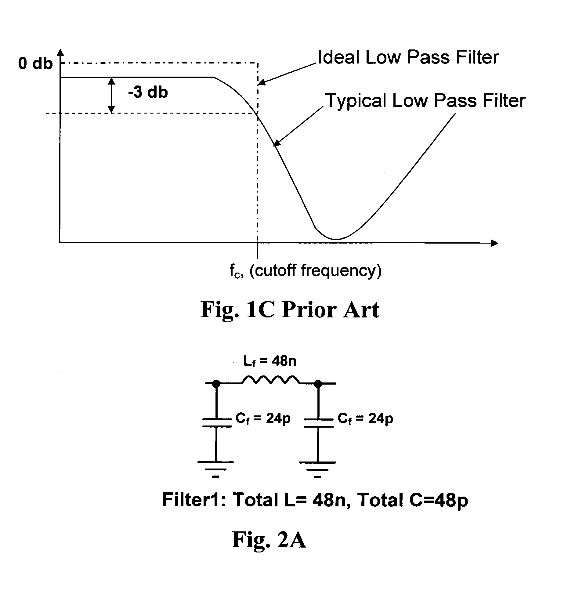
[0022]For better understanding of this invention, the descriptions of the FIGS. 2A to 2E below are provided as background reference information of the low pass filter implemented with distribute LC networks. FIGS. 2A to 2D are respectively circuit diagrams of low pass filters comprise inductors and capacitors. The total inductance is 48n and the total capacitance is 48p. In FIGS. 2B to 2D, instead of lumped LC network as shown in FIG. 2A, distributed inductors and capacitors are implemented to form the low pass filter while maintaining the total inductance and capacitance unchanged at 48n and 48p respectively. The distributed LC networks shown in FIGS. 2B to 2D have more poles compared to the lumped LC network when implemented for the low pass filter. FIG. 2E compares the insertion loss for each of the four low pass filters that are implemented with different numbers of LC networks as shown in FIGS. 2A to 2D respectively. FIG. 2E clearly illustrates that the distributed LC network w...


PUM


Abstract

An electronic circuit includes a filtering circuit implemented with a distributed inductor-and-capacitor (LC) network that includes metal oxide effect (MOS) trenches opened in a semiconductor substrate filled with dielectric material for functioning as capacitors for the distributed LC network. The electronic circuit further includes a transient voltage suppressing (TVS) circuit integrated with the filtering circuit that functions as a low pass filter wherein the TVS circuit includes a bipolar transistor triggered by a diode disposed in the semiconductor substrate. The distributed LC network further includes metal coils to function as inductors disposed on a top surface of the semiconductor electrically contacting the MOS trenches.

Description

BACKGROUND OF THE INVENTION[0001]1. Field of the Invention[0002]The invention relates generally to a circuit configuration and method of manufacture of a low pass filter. More particularly, this invention relates to an improved circuit configuration and method of manufacture of a low pass filters with improved characteristics of pass band attenuation having increased filter slope achieved by distributed inductor-capacitor networks by implementing trenched transient voltage suppressor (TVS) technologies.[0003]2. Description of the Relevant Art[0004]The low pass filters are commonly applied for filtering out radio frequency signals from audio / video / data line signals. Typically, electro-magnetic interference (EMI) filtering and electrostatic discharge (ESD) protection are combined into a single chip by using the capacitance of the Zener diodes to implement the filter as shown in FIG. 1A. Furthermore, filters implemented by combining the resistor-capacitor (RC) and inductor-capacitor (L...

Claims


Application Information

Patent Timeline
IPC IPC(8): H03H11/04H03H7/01H01L21/8222H01L21/82
CPCH01L23/60H01L23/66H01L27/0259H01L2924/0002H01L2924/00
Inventor BOBDE, MADHUR
Owner ALPHA & OMEGA SEMICON LTD
Why Eureka
Try Eureka