Optical apparatus of a stacked design, and method of producing same

a technology of optical apparatus and stacked design, which is applied in the direction of electrical apparatus, instruments, and spectrum investigation, etc., can solve the problems of inability to fully exploit the advantages of said technology, the signal intensity or signal sensitivity is not fully realized, and the cost of such an operation is generally high, so as to reduce the level of the effect of minimizing scattered light and/or extraneous light and higher system yield

Active Publication Date: 2009-10-22
FRAUNHOFER GESELLSCHAFT ZUR FOERDERUNG DER ANGEWANDTEN FORSCHUNG EV
View PDF11 Cites 129 Cited by
  • Summary
  • Abstract
  • Description
  • Claims
  • Application Information

AI Technical Summary

Benefits of technology

[0020]Embodiments in accordance with the invention are based on the core idea that the convoluted light path between the optical and the micromechanical substrates enables a compact and, therefore, inexpensive design, while the movable micromechanical element is arranged, in a protected manner, in an interior of the arrangement at the same time, and wherein the stacked design further results in a precise and simple alignment of the movable micromechanical element relative to the optical functional element. The movable micromechanical functional element is designed to influence radiation in a modulating (e.g. in a variably changeable) manner.
[0039]Some embodiments in accordance with the invention relate to the design and the production technology of spectrometers, produced in micro-technologies, for wavelength-resolved measurement of electromagnetic radiation, which include components for actively modulating this radiation. This refers, for example, to radiation of wavelengths starting with UV radiation and proceeding to visible radiation (VIS) and to IR radiation. The design of the system enables low-cost and simple production with a high level of adjustment accuracy due to the advantageous technological integration of optical, micromechanical and electronic components. The design of the spectrometer is implemented such that the (micro-)optical, mechanical, micromechanical and micro-electronic components are integrated on or in various substrates. The functional elements which may be produced by the same technology are integrated on a substrate in each case, which is why no change in existing technologies is necessary. Adjusting the various functional elements, which are arranged on different substrates in each case, is possible in a simple manner and with a high level of accuracy by exploiting the high level of evenness of the substrates, and by using adjusting marks, adjusting structures or integrated diffractive optical elements or modern means for aligning same. The unit which is fixed to form a stack (e.g. wafer stack) by a joining technique such as wafer bonding, gluing or soldering, for example, and / or by mechanical fixing connections such as clamping connections and / or screwed connections is diced into spectrometer modules by means of a separating method, such as sawing with a wafer saw, or laser cutting. By manufacturing many MOEMS spectrometer modules in parallel, efficient mass production of a hybrid overall system consisting of (micro-)optical, mechanical, micromechanical and / or (micro)electronic components, as has been common practice in microelectronics for a long time, is achieved.

Problems solved by technology

This conflicts with the high demands associated with the various assemblies.
With this spectrometer type, radiation impinging on a one-dimensional detector array is spectrally split up, as a result of which said systems have a limited spectral resolution and a limited spectral measuring range, and the multitude of detectors of a detector array lead to a deviation of the signal intensity, or signal sensitivity, on account of various levels of sensitivity and amplification.
However, the advantages of said technology cannot be fully exploited so far, since the savings in terms of the amount of work involved in the production of the individual components is compensated for by the more complicated adjustment and installation.
With spectrometers which are almost entirely built of discrete components, discrete optical, micromechanical, mechanical and electronic devices, which are manufactured in different processes, respectively, are combined into one overall system by means of adjustment and installation, which generally is costly.
Only one spectrometer module may be produced per operating cycle, as a result of which the production cost and, therefore, the total prices of these systems are high.
As a result, application of these systems on the mass market is limited.
Due to the components being shrunk, they exhibit a surface roughness and thermal deformation which is too high for optical components, and they therefore exhibit lower optical efficiency (diffraction efficiency grating, surface roughness, .
. . ), which results in a poorer signal / noise ratio, lower spectral resolution, and a poorer stray-light behavior.
Due to restrictions in the production by plastic injection molding, invariance toward environmental impacts cannot be achieved.
Due to the large tolerances, advantageous concepts for spectrometers comprising micromechanical components are difficult to put into practice.
The high manufacturing requirements placed upon the optical and mechanical components, in particular, considerably increase the cost of the production.
A specific technology which may be used for producing (micro-)optical, mechanical, micromechanical and microelectronic elements generally cannot be adapted at all or only with great difficulty, since said technology is determined by the respective specific requirements.
By joining, for example gluing, so-called wafer bonding (connecting disc-shaped substrates) or soldering the wafers or substrates in a clean-room atmosphere, a reduction of the dust particles within the spectrometer module may be achieved, among other things, which dust particles would result in poorer functioning of the system.

Method used


Image

  • Optical apparatus of a stacked design, and method of producing same
  • Optical apparatus of a stacked design, and method of producing same
  • Optical apparatus of a stacked design, and method of producing same

Examples


Embodiment Construction

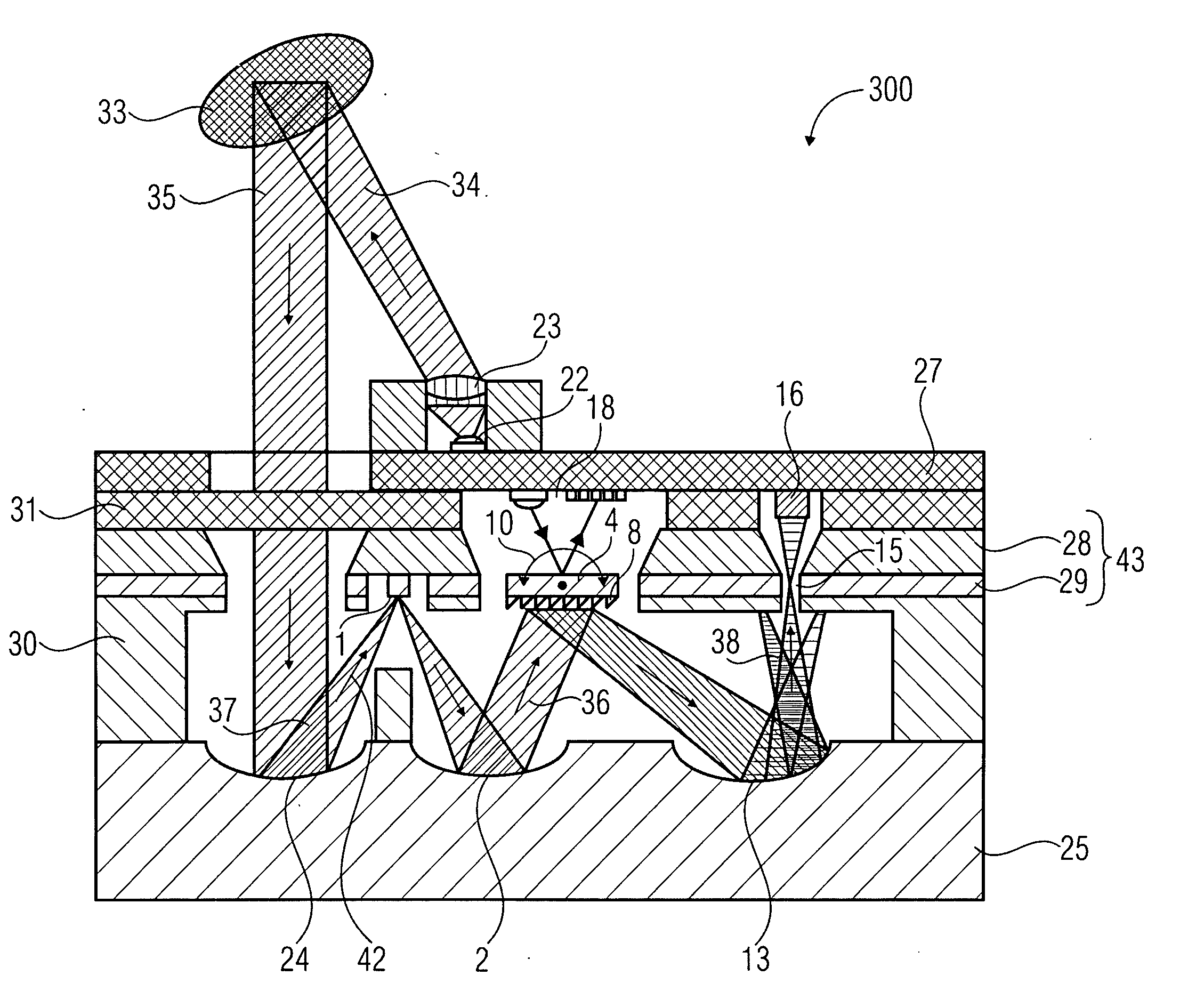
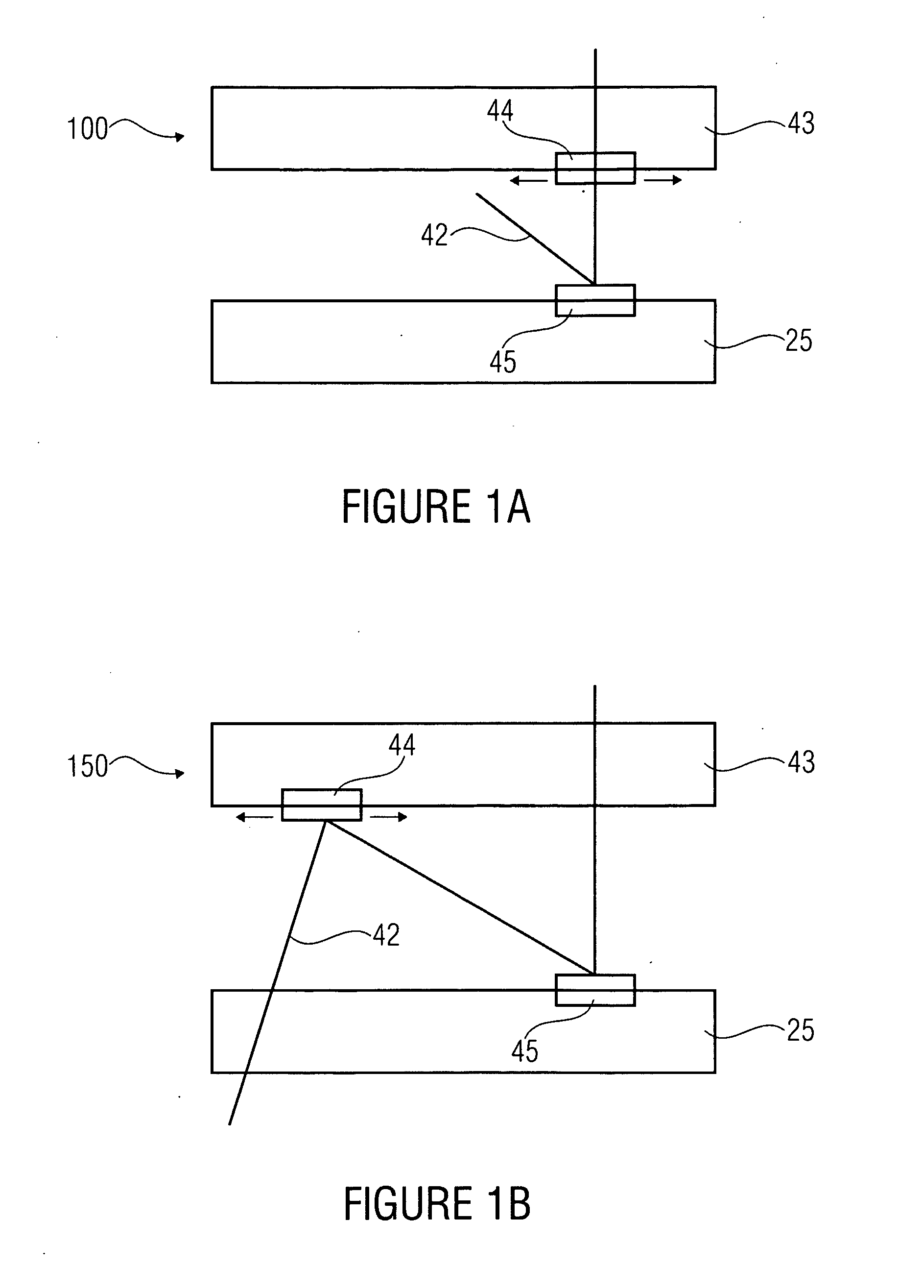
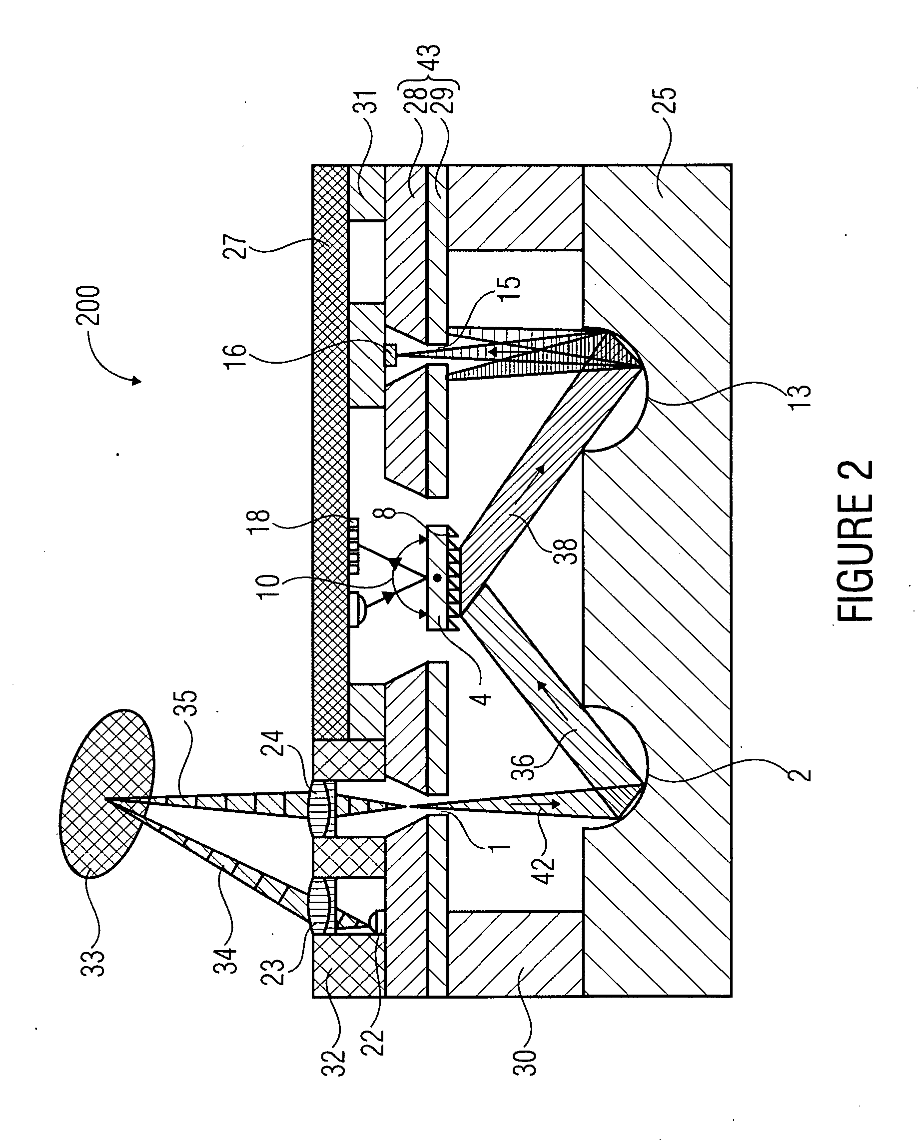
[0059]FIGS. 1A and 1B show schematic cross-sectional representations of an optical apparatus in accordance with embodiments of the invention. The optical apparatuses are designated by 100 and 150, respectively, in their entireties. The apparatuses, or the systems, are built in a stacked manner of a first substrate 25, also referred to as an optical substrate, and of a second substrate 43, also referred to as a micromechanical substrate, at least one optical functional element 45 being arranged in or on the optical substrate 25, and at least one movable micromechanical functional element 44 being arranged in or on the micromechanical substrate 43. The first substrate 25 and the second substrate 43 are connected to each other in a stacked manner such that a light path 42 exists which is convoluted between the first substrate 25 and the second substrate 43, at least one movable micromechanical functional element 44 and at least one optical functional element 45 being arranged in the li...


PUM

PropertyMeasurementUnit
distanceaaaaaaaaaa
sizesaaaaaaaaaa
transmissionaaaaaaaaaa

Abstract

An optical apparatus includes a first substrate including an optical functional element, and a second substrate including a movable micromechanical functional element, the first substrate and the second substrate being connected in a stacked manner, so that a light path exists which is convoluted between the first substrate and the second substrate, the movable micromechanical functional element and the optical functional element being arranged in the light path. In addition, a method of producing an optical apparatus includes producing a first substrate including an optical functional element, and producing a second substrate including a movable micromechanical functional element, as well as connecting the first and second substrates, so that a light path exists which is convoluted between the first and second substrates, the movable micromechanical functional element and the optical functional element being arranged in the light path.

Description

CROSS-REFERENCE TO RELATED APPLICATIONS[0001]This application claims priority from German Patent Application No. 102008019600.2, which was filed on Apr. 18, 2008 and is incorporated herein in its entirety by reference.[0002]Embodiments in accordance with the invention relate to an optical apparatus, also referred to below as an optical system or, generally, a system, of a stacked design which comprises an optical functional element and a movable micromechanical functional element, and to a method of producing such an optical apparatus.[0003]Some embodiments in accordance with the invention relate to MOEMS (micro-opto-electromechanical system) spectrometer modules which are integrated in a hybrid manner.BACKGROUND OF THE INVENTION[0004]Nowadays, spectrometers are employed, inter alia, for identifying materials or substances, such as for analyzing foodstuffs, in process measurement engineering for regulating and monitoring the composition of materials, and for quality control. The pre...

Claims


Application Information

Patent Timeline
Patent Type & Authority Applications(United States)
IPC IPC(8): G01J3/28G02F1/29H01L21/50
CPCG01J3/02G01J3/021G01J3/0256G01J3/0291G02B26/106G02B5/1828G02B26/08G02B26/0808G01J3/18
Inventor EGLOFF, THOMASKNOBBE, JENSGRUEGER, HEINRICH
Owner FRAUNHOFER GESELLSCHAFT ZUR FOERDERUNG DER ANGEWANDTEN FORSCHUNG EV
Why Eureka
Try Eureka