Optical information recording medium and method for manufacturing the same

Inactive Publication Date: 2009-10-22
PANASONIC CORP
View PDF17 Cites 7 Cited by
  • Summary
  • Abstract
  • Description
  • Claims
  • Application Information

AI Technical Summary

Benefits of technology

[0022]According to the present invention, it is possible to provide a high-capacity and low-cost optical information recording medium that can simultaneously achieve both a high transmittance and high signal quality, and achieve an excellent

Problems solved by technology

In this case, however, the jitter of recorded signals is disadvantageously low.
Therefore, it is difficult to select a material that is capable of reducing light absorption while securing heat radiation performance.
Also, in order to increase signal quality and reliability, an information layer typically includes multiple layers,

Method used


Image

  • Optical information recording medium and method for manufacturing the same
  • Optical information recording medium and method for manufacturing the same
  • Optical information recording medium and method for manufacturing the same

Examples


example 1

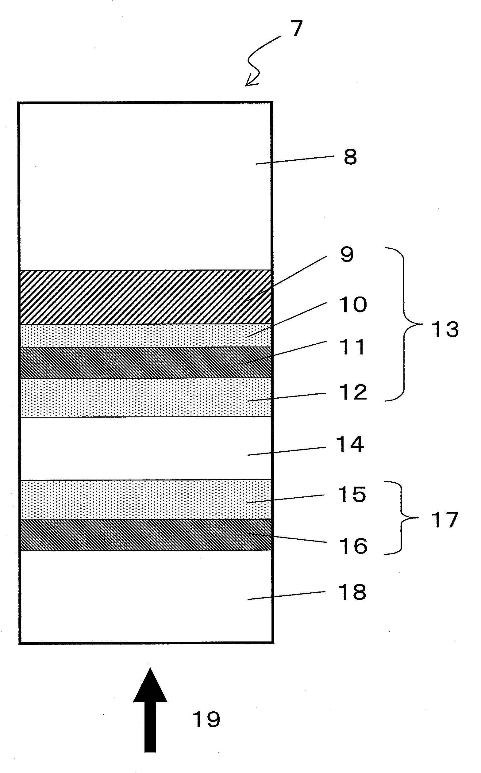
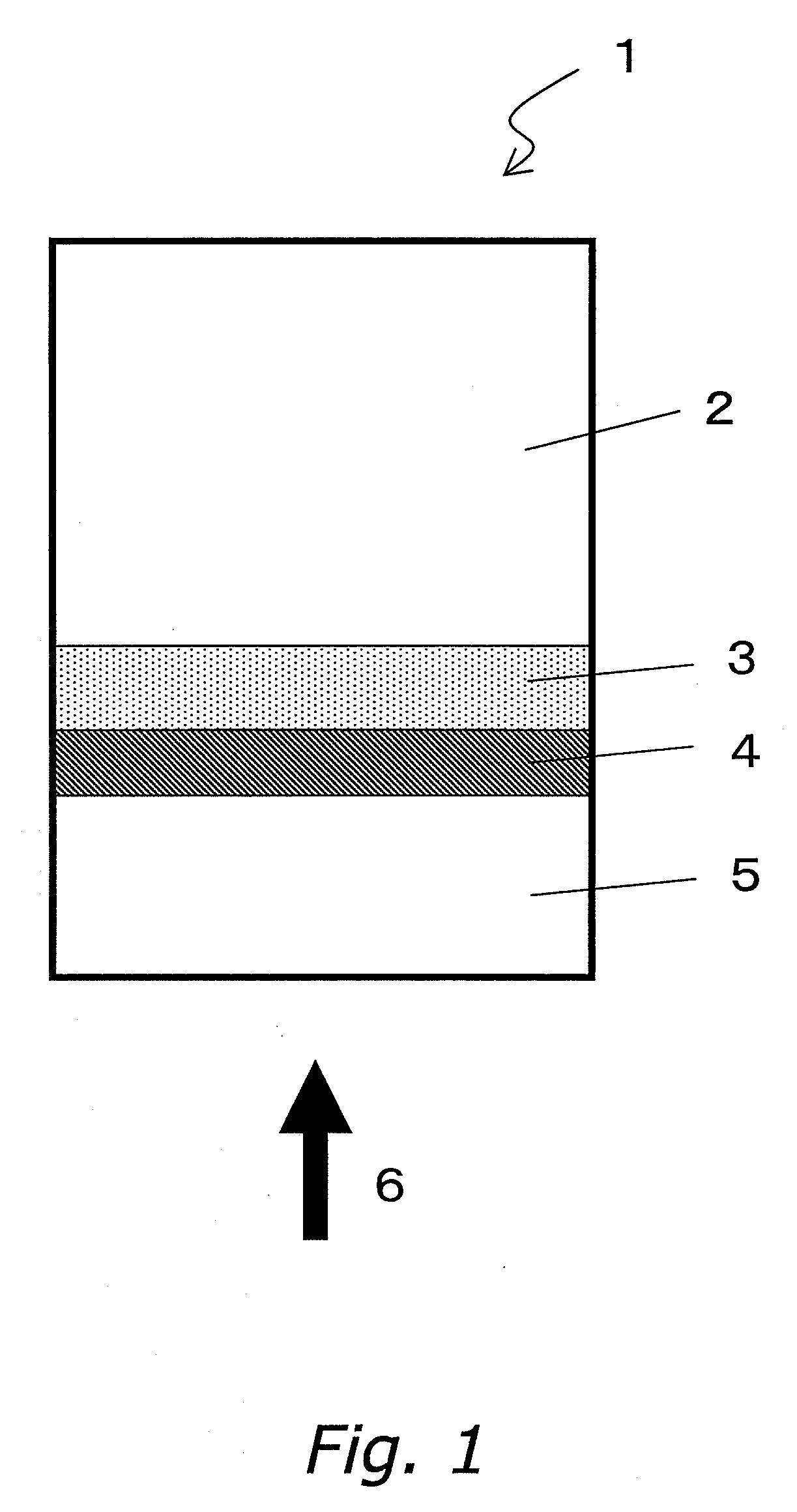
[0092]An optical information recording medium having the layer structure of FIG. 1 was fabricated, and the manufacture method will be described. Here, a dielectric layer is inserted between a recording layer and a light transparent layer so as to adjust optical characteristics to enable effective light absorption in an information layer.

[0093]A substrate was made of a polycarbonate resin. The substrate had a diameter of 12 cm, a thickness of 1.1 mm, a groove pitch of 0.32 μm, and a groove depth of 20 nm.

[0094]On a surface of the substrate in which a groove is formed, layers constituting a first information layer were formed by sputtering, one on the top of another in the following order. An AlN dielectric layer having a film thickness of 8 nm was formed using an AlN target: a Te—O—Pd recording layer having a film thickness of 6 nm was formed using a Te—O—Pd (atomicity ratio=37:53:10) target; a ZnS dielectric layer having a film thickness of 27 nm was formed using a ZnS target. A lig...

example 2

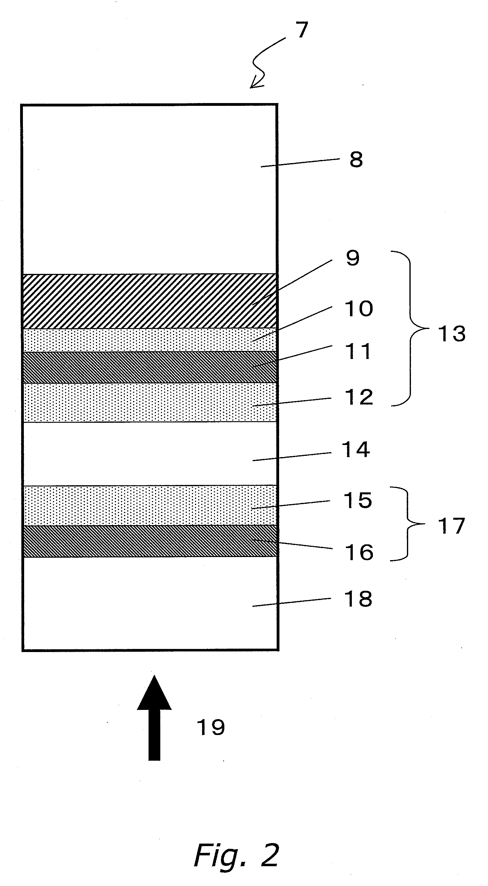
[0118]An optical information recording medium having the layer structure of FIG. 2 was fabricated, and the manufacture method will be described. Here, three kinds of media were fabricated and compared: (1) a dielectric layer of an information layer on the laser incident side of a two-layer medium was made of AlN having a thermal conductivity of 0.01 W / K·cm or more; (2) the dielectric layer was made of ZnS—SiO2 of 0.01 W / K·cm or less; and (3) a Ag alloy reflection layer and a conventional dielectric layer were used.

[0119]A substrate was made of a polycarbonate resin. The substrate had a diameter of 12 cm, a thickness of 1.1 mm, a groove pitch of 0.32 μm, and a groove depth of 20 nm.

[0120]On a surface of the substrate in which a groove is formed, layers constituting a first information layer were formed by sputtering in the following order: a AgPdCu reflection layer having a film thickness of 40 nm was formed using a AgPdCu (weight ratio=98.1: 0.9:1.0) target; a ZrO2—SiO2—Cr2O3—LaF3 d...

example 3

[0129]An optical information recording medium having the layer structure of FIG. 3 (n=4) was fabricated, and the manufacture method will be described. A substrate was made of a polycarbonate resin. The substrate had a diameter of 12 cm, a thickness of 1.1 mm, a groove pitch of 0.32 μm, and a groove depth of 20 nm.

[0130]On a surface of the substrate in which a groove is formed, layers constituting a first information layer were formed by sputtering in the following order: a AgPdCu reflection layer having a film thickness of 40 nm was formed using a AgPdCu (weight ratio=98.1:0.9:1.0) target; a ZrO2—SiO2—Cr2O3—LaF3 dielectric layer having a film thickness of 20 nm was formed using a ZrO2—SiO2—Cr2O3—LaF3 (molecularity ratio=23:23:31:23) target; a Te—O—Pd recording layer having a film thickness of 20 nm was formed using a Te—O—Pd (atomicity ratio=37:53:10) target; and a ZnS—SiO2 dielectric layer having a film thickness of 30 nm was formed using a ZnS—SiO2 (molecularity ratio=80:20) targe...


PUM

PropertyMeasurementUnit
Thicknessaaaaaaaaaa
Thicknessaaaaaaaaaa
Thicknessaaaaaaaaaa

Abstract

An optical information recording medium that can simultaneously achieve both a high transmittance and high signal quality of an information layer, improve the reliability of long-term conservation, and reduce the manufacturing cost, and a manufacturing method thereof are provided. To achieve this, according to the present invention, in an optical information recording medium comprising at least one information layer on a substrate, at least one of the information layers has a recording layer and a dielectric layer, the recording layer contains Te, O, and M (M is one or a plurality of elements selected from Au, Pd, and Pt) as major components, the dielectric layer has a thermal conductivity of 0.01 W/K·cm or more, and the dielectric layer has an extinction coefficient of 0 through 1.0 inclusive.

Description

TECHNICAL FIELD[0001]The present invention relates to an optical information recording medium that makes it possible to record and reproduce an information signal by irradiating a thin film formed on a substrate with a high-energy light beam, such as a laser beam or the like, and a method for manufacturing the same.BACKGROUND ART[0002]Phase-change type recording media are known as media that makes it possible to record and reproduce a large amount of information with high speed. In phase-change type recording media, recording is performed by utilizing a phenomenon that a recording material thereof is changed to an optically distinguishable state due to heat generated by locally irradiating the recording material with laser light. Phase-change type recording media enable random access as required and have excellent portability, and therefore, are becoming more and more important in recent years. For example, there is an increasing demand in various fields, such as recording or conser...

Claims


Application Information

Patent Timeline
IPC IPC(8): B32B3/02B05D5/06G11B7/24G11B7/24035G11B7/24038G11B7/24047G11B7/243G11B7/2433G11B7/2437G11B7/254G11B7/257G11B7/258G11B7/2585G11B7/259G11B7/2595
CPCG11B7/24038G11B7/243G11B7/257G11B2007/24306G11B2007/24308G11B2007/24316Y10T428/21G11B2007/25706G11B2007/25708G11B2007/2571G11B2007/25711G11B2007/25713G11B2007/25715G11B2007/2432G11B7/2433
Inventor HABUTA, HARUHIKOTOMIYAMA, MORIOKITAURA, HIDEKI
Owner PANASONIC CORP
Why Eureka
Try Eureka