Three-dimensional circuit board and its manufacturing method

a three-dimensional circuit board and manufacturing method technology, applied in the direction of circuit masks, conductive pattern formation, lithography/patterning, etc., can solve the problems of increasing connection resistance, limited three-dimensional wiring of high density, and difficult to dramatically enhance the performance of the existing method from the standpoint of cost and technology, so as to achieve high reliability and high density

Inactive Publication Date: 2009-10-29
PANASONIC CORP
View PDF6 Cites 21 Cited by
  • Summary
  • Abstract
  • Description
  • Claims
  • Application Information

AI Technical Summary

Benefits of technology

[0040]This configuration realizes a three-dimensional circuit board free from land and connection interface, and having a wiring-electrode group consisting of a first wiring-electrode group and a second wiring-electrode of high density and high reliability.
[0042]This method easily manufactures a three-dimensional circuit board free from land and connection interface, and having a wiring-electrode of high density and high reliability continuously in batch process.

Problems solved by technology

However, even in a highly integrated semiconductor chip, it is now becoming difficult to enhance the performance dramatically in the existing method from the viewpoint of cost and technology.
Besides, since conductor patterns 4020 can be formed only on both side of resin films, three-dimensional wiring of high density is limited.
Since conductive vias 4030 and conductor patterns 4020 are connected by compressing or bonding, due to entry of foreign matter or forming of oxide film on the connection interface, the connection resistance may be increased, or the connection reliability may not be satisfactory.
When a plurality of resin films are laminated and integrated, due to remaining bubbles or the like, peeling is likely to occur, and the reliability may be inferior.
However, in this wiring board, too, since the conductor patterns are larger than the shape of conductive vias, conductor patterns of fine pitches cannot be formed.
Besides, since the conductor patterns are formed on the flatly formed electric insulating layer, conductor patterns cannot be formed at desired positions.
Yet, since the conductor patterns, conductive vias, and electric insulating layers are formed in separate processes in each layer, the productivity is lowered, and the reliability is connection is not satisfactory between layers of conductor patterns and conductive vias.
It is hence difficult to form electric circuit patterns having a three-dimensional structure.
Moreover, since the electric circuit patterns are formed by etching, it is difficult to form finely in steps of three-dimensional structure, and the productivity is lower.

Method used


Image

  • Three-dimensional circuit board and its manufacturing method
  • Three-dimensional circuit board and its manufacturing method
  • Three-dimensional circuit board and its manufacturing method

Examples


first preferred embodiment

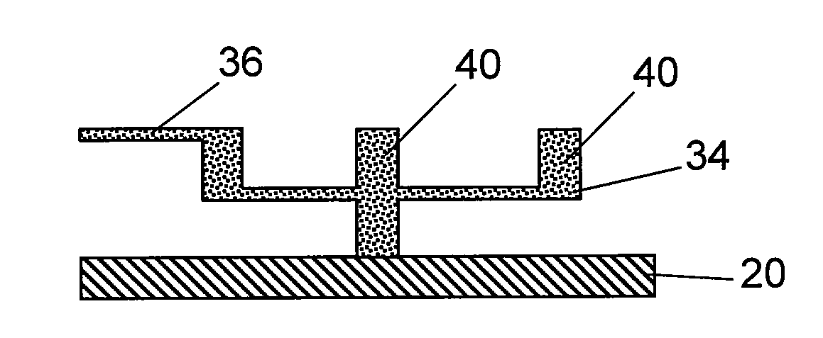
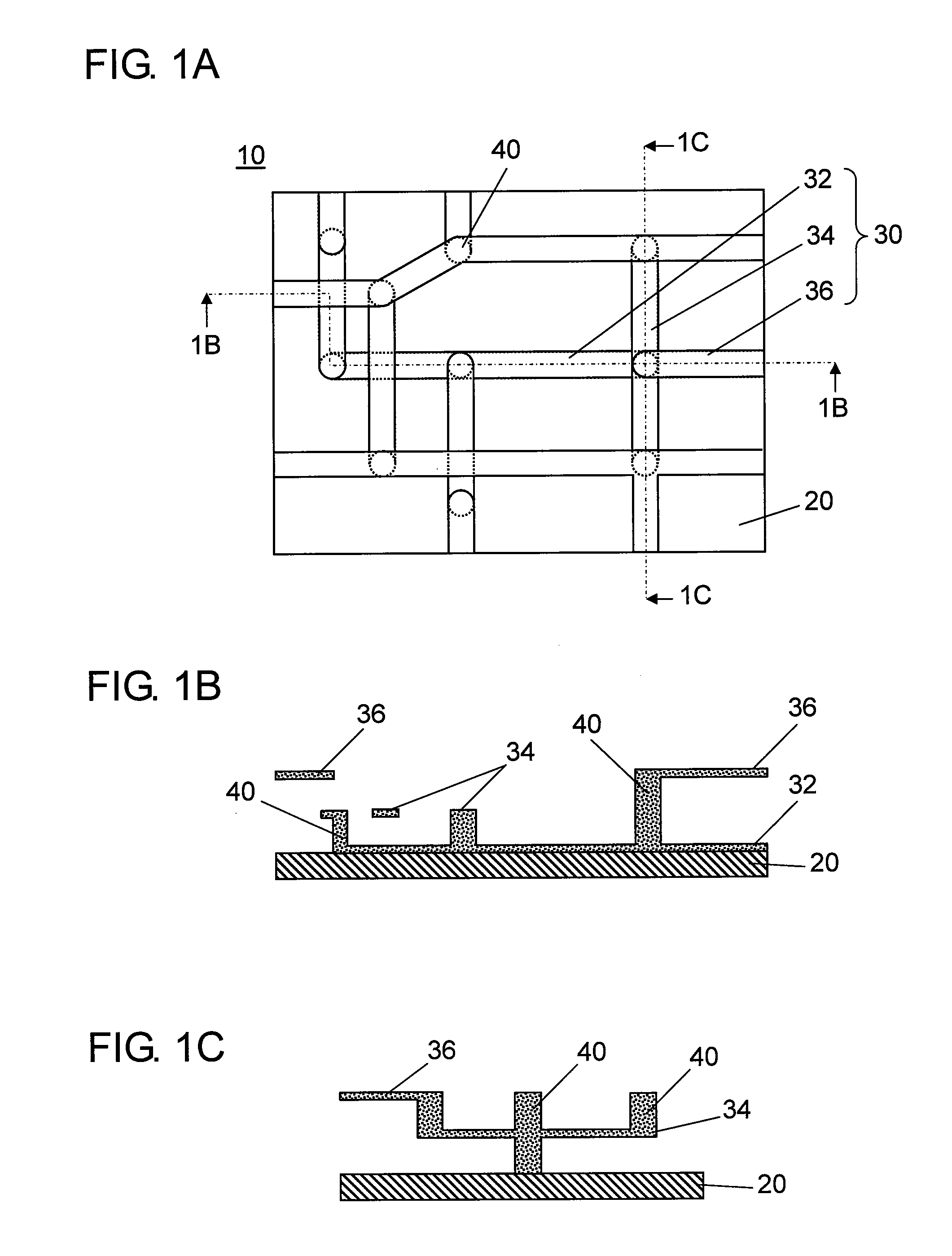
[0187]FIG. 1A is a partial plan view schematically showing a three-dimensional circuit board in a first preferred embodiment of the present invention, FIG. 1B is a sectional view along line 1B-1B in FIG. 1A, and FIG. 1C is a sectional view along line 1C-1C in FIG. 1A.

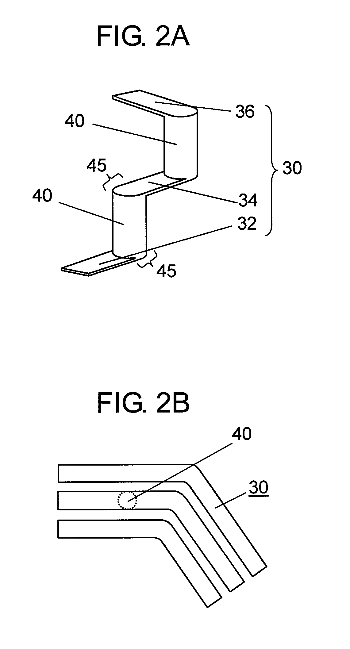
[0188]As shown in FIG. 1A to FIG. 1C, three-dimensional circuit board 10 has a wiring-electrode group formed three-dimensionally by a conductive photosetting resin made of a photosetting resin containing conductive filler such as silver, gold, copper, silver, or palladium particles, provided at least on one side of board 20 made of polyethylene terephthalate (PET), polyethylene naphthalate, polyimide, glass epoxy resin, silicon, or glass. For the ease of understanding of the wiring-electrode group shown in FIG. 1A, the one shown in band shape is called first wiring-electrode group 30, and the other formed in circular shape is called second wiring-electrode 40. Second wiring-electrode 40 has a same action as a conductive...

second preferred embodiment

[0224]FIG. 8A is a partial sectional view schematically showing a three-dimensional circuit board in a second preferred embodiment of the present invention, and FIG. 8B is a partial sectional view schematically showing another example of three-dimensional circuit board in the second preferred embodiment of the present invention.

[0225]As shown in FIG. 8A, three-dimensional circuit board 200 in the second preferred embodiment of the present invention differs from three-dimensional circuit board 10 in the first preferred embodiment in that it has first wiring-electrode group 230 composed of first wiring-electrode 235 provided at an arbitrary angle to the horizontal direction of board 220 and first wiring-electrode 238 differing in sectional shape, and second wiring-electrode group 240 composed of second wiring-electrode 244 provided in an oblique direction. Herein, an arbitrary angle to the horizontal direction means that at least a part of the first wiring-electrode group or second wi...

third preferred embodiment

[0239]FIG. 9A is a partial plan view schematically showing a three-dimensional circuit board in a third preferred embodiment of the present invention, FIG. 9B is a sectional view along line 9B-9B in FIG. 9A, and FIG. 9C is a sectional view along line 9C-9C in FIG. 9A.

[0240]As shown in FIG. 9A, three-dimensional circuit board 300 is different from three-dimensional circuit board 60 in another example of the first preferred embodiment in that dummy electrodes 330, 340 not connecting with other first wiring-electrode group or second wiring-electrode are provided, for example, in first wiring-electrode 310, in the case of connection electrode 320 formed in a state floating in air, for holding them, when one end is a free end or in a process of forming a three-dimensional wiring-electrode group.

[0241]That is, as shown in FIG. 9B, for example, connection electrode 320 for connecting only between the electronic components to be mounted on three-dimensional circuit board 300 is not usually ...


PUM

PropertyMeasurementUnit
degree of freedomaaaaaaaaaa
thicknessaaaaaaaaaa
thicknessaaaaaaaaaa

Abstract

A three-dimensional circuit board is formed by comprising a board, a first wiring-electrode group provided on a plurality of steps above the board, and a second wiring-electrode connected to the first wiring-electrode group at least in an altitude direction, in which at least a connecting portion between the first wiring-electrode group and the second wiring-electrode is integrated in a continuously identical shape.

Description

TECHNICAL FIELD[0001]The present invention relates to a three-dimensional circuit board for realize three-dimensional wiring of high density, and its manufacturing method.BACKGROUND ART[0002]Recently, a portable telephone or a personal digital terminal is rapidly developing into a comprehensive information appliance by incorporating various functions. To realize multiple functions in a limited volume, the primary demands are reduction of size and enhancement of performance of various devices such as semiconductor chips. However, even in a highly integrated semiconductor chip, it is now becoming difficult to enhance the performance dramatically in the existing method from the viewpoint of cost and technology.[0003]At the present, therefore, there is a mounting demand for high-density mounting technology for housing devices in a compact size.[0004]For higher integration of devices, evolution from two-dimensional wiring to three-dimensional wiring is demanded to satisfy the requests fo...

Claims


Application Information

Patent Timeline
Patent Type & Authority Applications(United States)
IPC IPC(8): H05K1/00H05K3/00
CPCH05K3/0082H05K3/207H05K3/4069H05K3/4647Y10T29/49124H05K2201/0347H05K2203/0514H05K2203/056H05K2203/107H05K3/4664H01L2224/16227H01L2924/19041H01L2924/19105H05K1/02H05K3/00H05K3/10H05K3/20H05K1/03
Inventor SAKURAI, DAISUKEYAGI, YOSHIHIKO
Owner PANASONIC CORP
Why Eureka
Try Eureka