Semiconductor device and method for manufacturing semiconductor device

a semiconductor and semiconductor technology, applied in the direction of semiconductor/solid-state device manufacturing, semiconductor devices, semiconductor devices, etc., can solve the problems of easy damage to the semiconductor device, high cost of the dicer (a dicing blade) or the like used as a scribing device, and easy identification. , the effect of reducing misidentification even in automatic operation

Inactive Publication Date: 2009-10-29
SEMICON ENERGY LAB CO LTD
View PDF36 Cites 86 Cited by
  • Summary
  • Abstract
  • Description
  • Claims
  • Application Information

AI Technical Summary

Benefits of technology

[0028]In the above structure, an embodiment of the semiconductor device may be that the side surface of the light-transmitting substrate in contact with the light-transmitting resin layer is a curved surface which spreads toward the bottom. The light-transmitting substrate has the curved side surface which spreads toward the bottom, whereby the light-transmitting resin layer can be provided so as to cover the curved side surface. Further, a bottom surface and a top surface of the light-transmitting substrate are quadrangles, and the area of the bottom surface is larger than that of the top surface. In the light-transmitting substrate of a semiconductor device in this specification, the surface in contact with a light-transmitting resin layer is referred to as a top surface, and the surface provided with the semiconductor integrated circuit portion is referred to as a bottom surface. In the case where the area of the bottom surface of the light-transmitting substrate is larger than that of the top surface of the light-transmitting substrate, the light-transmitting resin layer can be formed on a side surface in the region where the bottom surface and the top surface do not overlap with each other so as to cover the light-transmitting substrate.
[0029]As thus described, the semiconductor device of the present invention has a complicated shape; therefore, top and bottom sides of the semiconductor device can be easily distinguished. Thus, misidentification even in an automatic operation by a machine can be reduced.
[0030]Further, the semiconductor integrated circuit includes an amplifier circuit for amplifying the output of the photoelectric conversion element. The photoelectric conversion element may have a layered structure in which a p-type semiconductor layer, an i-type semiconductor layer, and an n-type semiconductor layer are stacked.
[0031]In this specification, an i-type semiconductor corresponds to the semiconductor in which the concentration of an impurity which imparts p-type or n-type conductivity is 1×1020 cm−3 or less; the concentration of oxygen and nitrogen is 1×1020 cm−3 or less; and photoconductivity exceeds dark conductivity by 100 times or more. The i-type semiconductor may include an impurity element which belongs to Group 13 or Group 15 of the periodic table. That is, the i-type semiconductor has weak n-type electric c...

Problems solved by technology

However, a semiconductor device is likely to be damaged due to external stress such as pressure applied in any of steps for manufacturing a semiconductor device except a step of cutting a substrate, or a step of inspecting the semiconductor device.
The thinner and the weaker a substrate is, the more frequent...

Method used


Image

  • Semiconductor device and method for manufacturing semiconductor device
  • Semiconductor device and method for manufacturing semiconductor device
  • Semiconductor device and method for manufacturing semiconductor device

Examples


embodiment 1

[0060]In this embodiment, a semiconductor device for realizing reduction in thickness and size and a method for manufacturing the semiconductor device with high yield are described in detail with reference to FIGS. 1A and 1B, FIGS. 2A and 2B, FIGS. 3A to 3F, FIGS. 4A and 4B, FIGS. 5A to 5D, FIGS. 6A to 6C, FIGS. 7A and 7B, and FIGS. 8A and 8B.

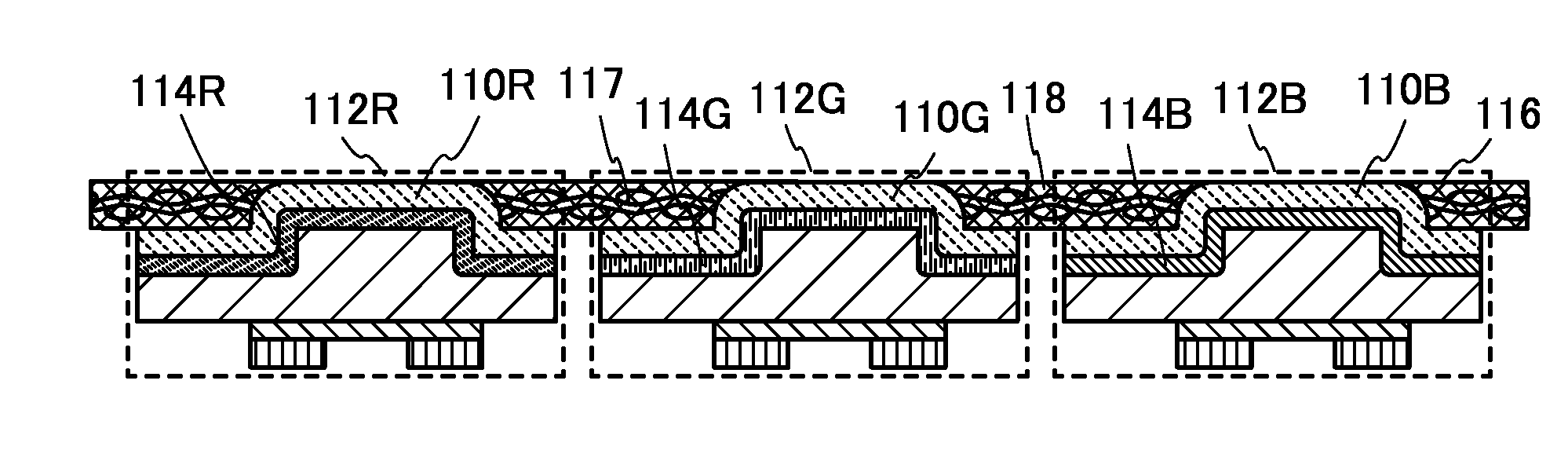
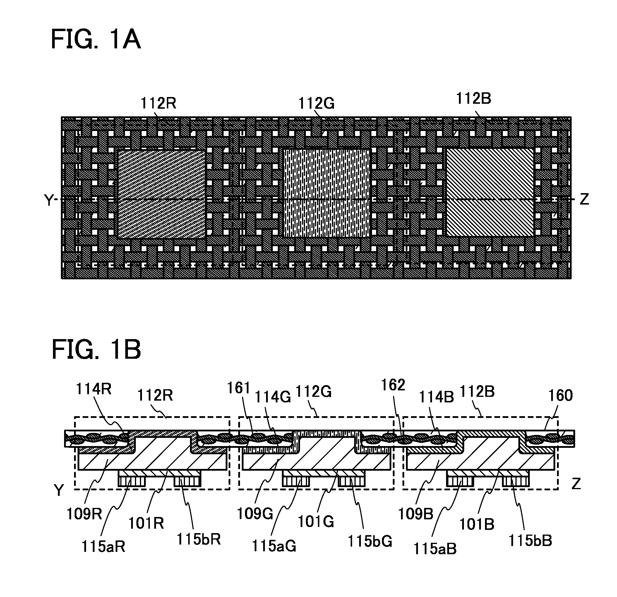
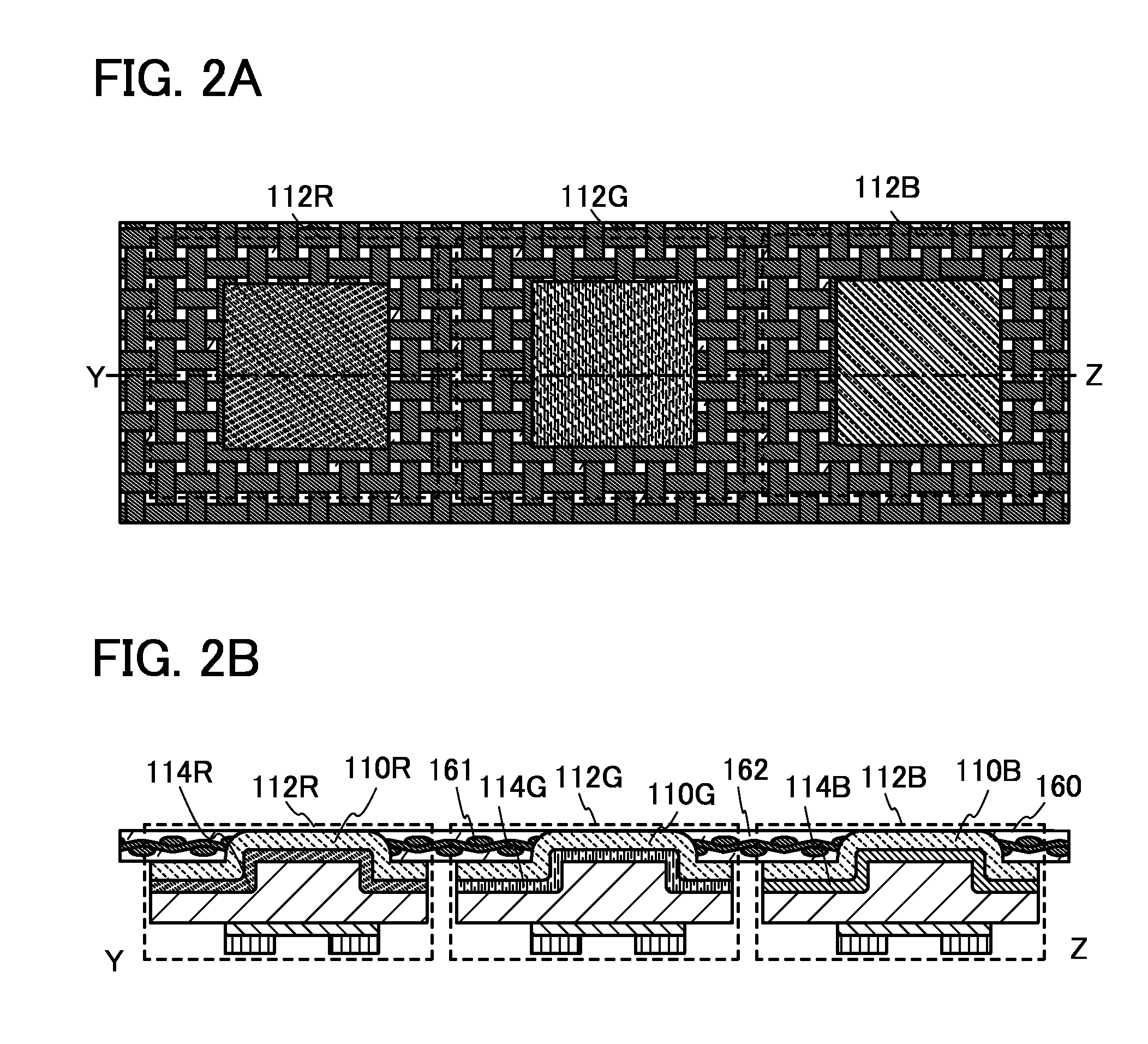
[0061]FIGS. 1A and 1B illustrate a semiconductor device of this embodiment. FIG. 1A is a plan view of the semiconductor device, and FIG. 1B is a cross-sectional view along Y-Z in FIG. 1A.

[0062]The semiconductor device in FIGS. 1A and 1B has a structure in which a semiconductor integrated circuit 112R, a semiconductor integrated circuit 112G, and a semiconductor integrated circuit 112B are bonded to a structure body 160 in which a fibrous body 161 is impregnated with an organic resin 162. The semiconductor integrated circuit 112R, the semiconductor integrated circuit 112G, and the semiconductor integrated circuit 112B are provided with terminal ...

embodiment 2

[0207]For a semiconductor device according to an embodiment of the present invention, any of a variety of forms of field effect transistors can be used as a semiconductor element included in a semiconductor integrated circuit portion. In this embodiment, a field effect transistor including a single crystal semiconductor layer is described in detail as a semiconductor element.

[0208]A method in which a single crystal semiconductor layer made from a single crystal semiconductor substrate is provided over a light-transmitting substrate and a semiconductor element included in a semiconductor integrated circuit portion is formed is described below with reference to FIGS. 15A to 15D and FIGS. 16A to 16C.

[0209]A single crystal semiconductor substrate 1108 illustrated in FIG. 15A is cleaned, and is irradiated with ions accelerated by an electric field to a predetermined depth from the surface to form an embrittlement layer 1110. Ion irradiation is performed in consideration of the thickness ...

embodiment 3

[0273]This embodiment describes an example of steps of bonding a single crystal semiconductor layer from a single crystal semiconductor substrate to a light-transmitting substrate, which are different from those in Embodiment 2. Accordingly, description of the same portion or a portion having a similar function to the portion in Embodiment 2 is omitted.

[0274]First, processing on the single crystal substrate side is described. In this embodiment, a single crystal semiconductor substrate is degreased and cleaned to remove an oxide film on the surface, and thermal oxidation is performed. As thermal oxidation, oxidation in an oxidizing atmosphere to which halogen is added is preferably performed. For example, heat treatment is performed at a temperature of 700° C. or higher in an atmosphere containing HCl at 0.5 to 10 volume % (preferably 3 volume %) with respect to oxygen. Thermal oxidation is preferably performed at a temperature of 950 to 1100° C. The processing time may be 0.1 to 6 ...


PUM


Abstract

A semiconductor device includes a plurality of semiconductor integrated circuits bonded to a structure body in which a fibrous body is impregnated with an organic resin. The plurality of semiconductor integrated circuits are provided at openings formed in the structure body and each include a photoelectric conversion element, a light-transmitting substrate which has stepped sides and in which the width of the projected section on a first surface side is smaller than that of a second surface, a semiconductor integrated circuit portion provided on the second surface of the light-transmitting substrate, and a chromatic color light-transmitting resin layer which covers the first surface and part of side surfaces of the light-transmitting substrate. The plurality of semiconductor integrated circuits include the chromatic color light-transmitting resin layers of different colors.

Description

BACKGROUND OF THE INVENTION[0001]1. Field of the Invention[0002]The present invention relates to a semiconductor device and a method for manufacturing a semiconductor device. In particular, the present invention relates to a semiconductor device including a photoelectric conversion element.[0003]2. Description of the Related Art[0004]Among a variety of sensors, sensors which detect visible light with a wavelength of 400 to 700 nm are referred to as optical sensors or visible light sensors. Optical sensors or visible light sensors are known to be used for, for example, detecting optical signals to read data, detecting ambient brightness to control operation of electronic appliances, and the like.[0005]For example, in cellular phones or television units, optical sensors are used for adjusting the luminance of display screens in accordance with the ambient brightness of places where they are set.[0006]Such a semiconductor device typified by the optical sensor or the visible light senso...

Claims


Application Information

Patent Timeline
IPC IPC(8): H01L31/02H01L21/50
CPCH01L27/14625H01L31/075H01L27/14806H01L27/1214H01L27/1218H01L27/14603
Inventor TAKAHASHI, HIDEKAZUYAMADA, DAIKIMONMA, YOHEIIGUCHI, TAKAHIROADACHI, HIROKIYAMAZAKI, SHUNPEI
Owner SEMICON ENERGY LAB CO LTD
Why Eureka
Try Eureka