

Organic light emitting device and fabrication method thereof
a light-emitting device and organic technology, applied in the direction of organic semiconductor devices, discharge tubes/lamp details, discharge tubes luminescnet screens, etc., can solve the problems of low luminance and efficiency, high toxicity, low voltage of organic light-emitting devices, etc., to reduce the electron injection barrier, the effect of high efficiency and low toxicity
- Summary
- Abstract
- Description
- Claims
- Application Information
AI Technical Summary
Benefits of technology
Problems solved by technology
Method used
Image

Examples
embodiment 1
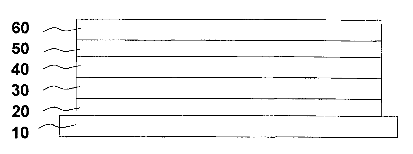
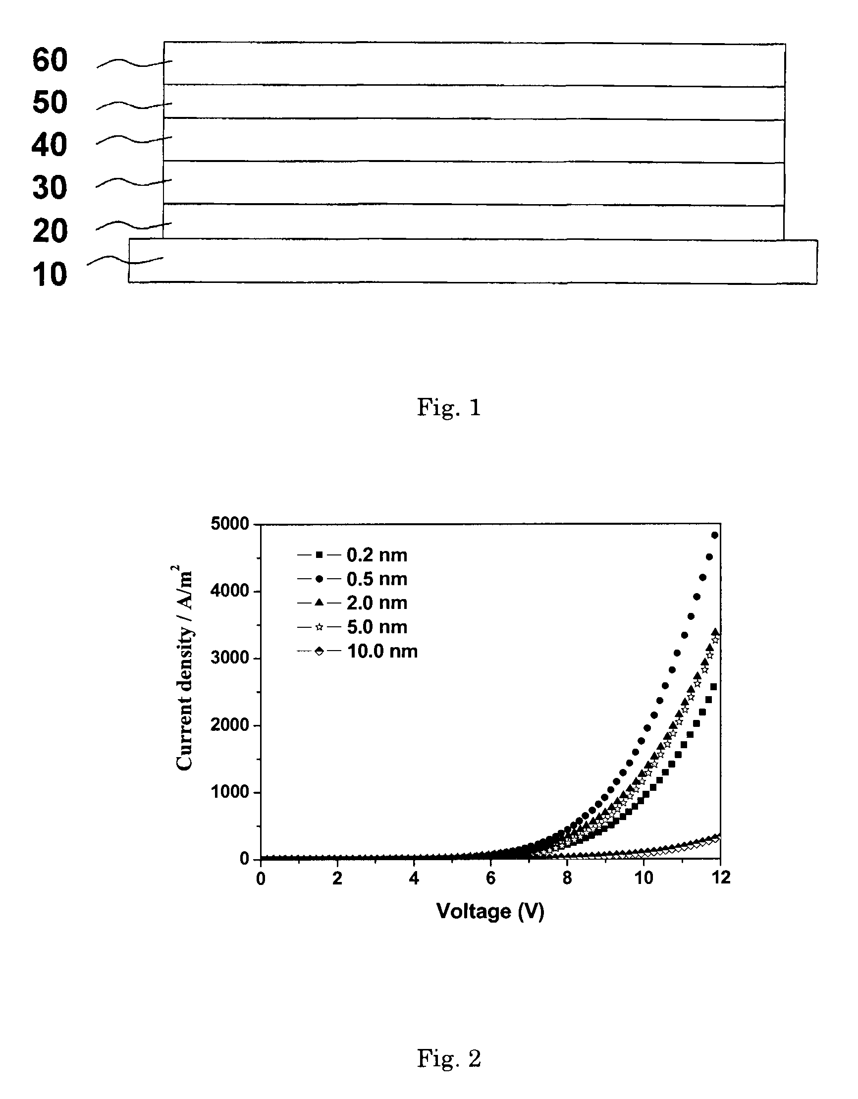
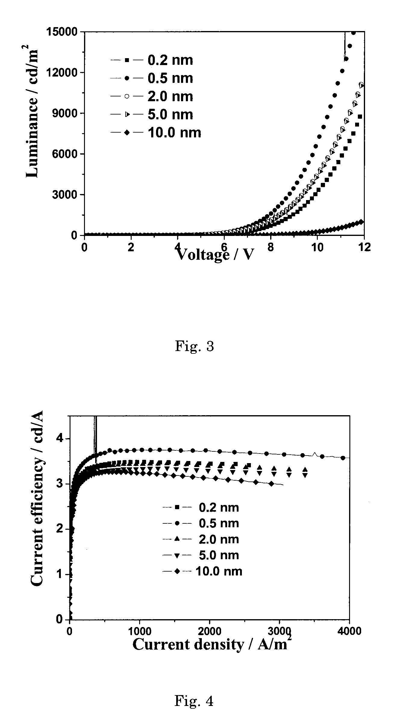
[0038]Refer to FIG. 1, which is a cross-sectional view of a structure of an organic light emitting device of the present embodiment. The organic light emitting device comprises a substrate 10, an anode layer 20, a hole transport layer 30, a light emitting layer 40, a cathode modification layer 50 and a cathode layer 60. The structure of the organic light emitting device of the embodiment of the invention is as follows:
[0039]glass substrate / ITO / NPB(50 nm) / Alq3(70 nm) / KBH4(0.2 nm) / Al(150 nm)
[0040]1) Fabrication of the Organic Light Emitting Layer
[0041]A pre-treated glass substrate is placed in a vacuum chamber. The chamber is evacuated to a pressure of 1×10⁻³ Pa. Ahole transport material of NPB is evaporated with an evaporation rate of 0.1 nm / s and a thickness of 50 nm. Alq3 is evaporated on the hole injection layer as the light emitting layer and the electron transport layer of the device with a thickness of 70 nm.
[0042]The glass substrate comprises an ITO (Indium Tin Oxide) film and...
embodiment 2
[0048]Refer to FIG. 1, which is a cross-sectional view of a structure of an organic light emitting device of the present embodiment. The organic light emitting device comprises a substrate 10, an anode layer 20, a hole transport layer 30, a light emitting layer 40, a cathode modification layer 50 and a cathode layer 60. The structure of the organic light emitting device in this embodiment of the invention is as follows:
[0049]glass substrate / ITO / NPB(50 nm) / Alq3(70 nm) / KBH4(0.5 nm) / Al(150 nm)
[0050]The method of fabricating the organic light emitting device is similar to that mentioned in embodiment 1. The difference therebetween lies in that a KBH4 layer with a thickness of 0.5 nm is fabricated after fabricating the electron transport layer.
embodiment 3
[0051]Refer to FIG. 1, which is a cross-sectional view of a structure of an organic light emitting device of the present embodiment. The organic light emitting device comprises a substrate 10, an anode layer 20, a hole transport layer 30, a light emitting layer 40, a cathode modification layer 50 and a cathode layer 60. The structure of the organic light emitting device in this embodiment of the invention is as follows:
[0052]glass substrate / ITO / NPB(50 nm) / Alq3(70 nm) / KBH4(2.0 nm) / Al(150 nm)
[0053]The method of fabricating the organic light emitting device is similar to that mentioned in embodiment 1. The difference therebetween lies in that a KBH4 layer with a thickness of 2.0 nm is fabricated after fabricating the electron transport layer.
PUM
 Abstract
Description
Claims
Application Information