Selective cobalt deposition on copper surfaces

a cobalt deposition and copper surface technology, applied in the direction of chemical vapor deposition coating, coating, plasma technique, etc., can solve the problems reducing the probability of errors, so as to achieve the effect of increasing the probability of errors

Inactive Publication Date: 2009-10-29
APPLIED MATERIALS INC
View PDF53 Cites 423 Cited by
  • Summary
  • Abstract
  • Description
  • Claims
  • Application Information

AI Technical Summary

Benefits of technology

[0009]Embodiments of the invention provide processes to selectively form a cobalt layer on a copper surface over exposed dielectric surfaces. In one embodiment, a method for capping a copper surface on a substrate is provided which includes positioning a substrate within a processing chamber, wherein the substrate contains a contaminated copper surface and a dielectric surface, exposing the contaminated...

Problems solved by technology

Filling the features without creating voids or deforming the feature geometry is more difficult when the features have higher aspect ratios.
Reliable formation of interconnects is also more difficult as manufacturers strive to increase circuit density and quality.
Each processing method may increase the likelihood of errors such as copper diffusion across boundary regions, copper crystalline structure deformation, and dewetting.
These options are costly or only partially effective or both.
The stress migrat...

Method used


Image

  • Selective cobalt deposition on copper surfaces
  • Selective cobalt deposition on copper surfaces
  • Selective cobalt deposition on copper surfaces

Examples


Embodiment Construction

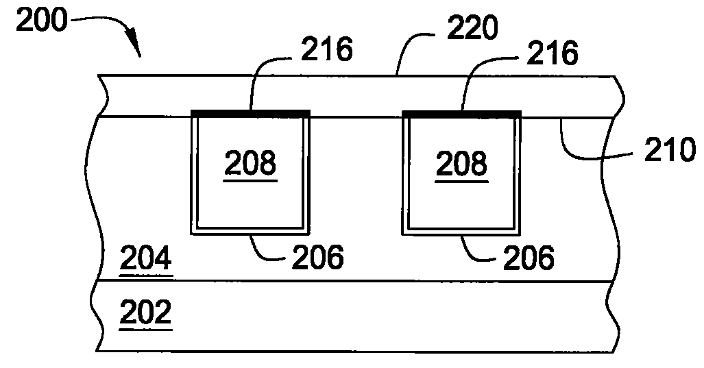
[0024]Embodiments of the invention provide a method that utilizes a cobalt capping layer or material to prevent copper diffusion and dewetting in interconnect boundary regions. The transition metal, for example, cobalt, improves copper boundary region properties to promote adhesion, decrease diffusion and agglomeration, and encourage uniform roughness and wetting of the substrate surface during processing. Embodiments provide that a cobalt capping layer may be selectively deposited on a copper contact or surface on a substrate while leaving exposed dielectric surfaces on the substrate.

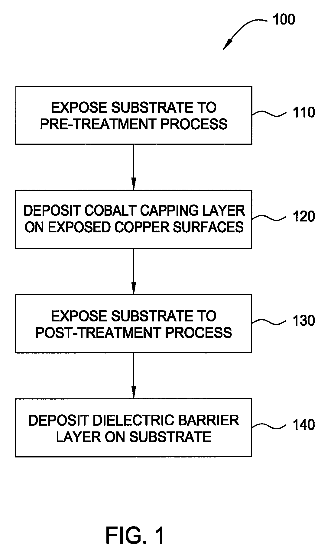
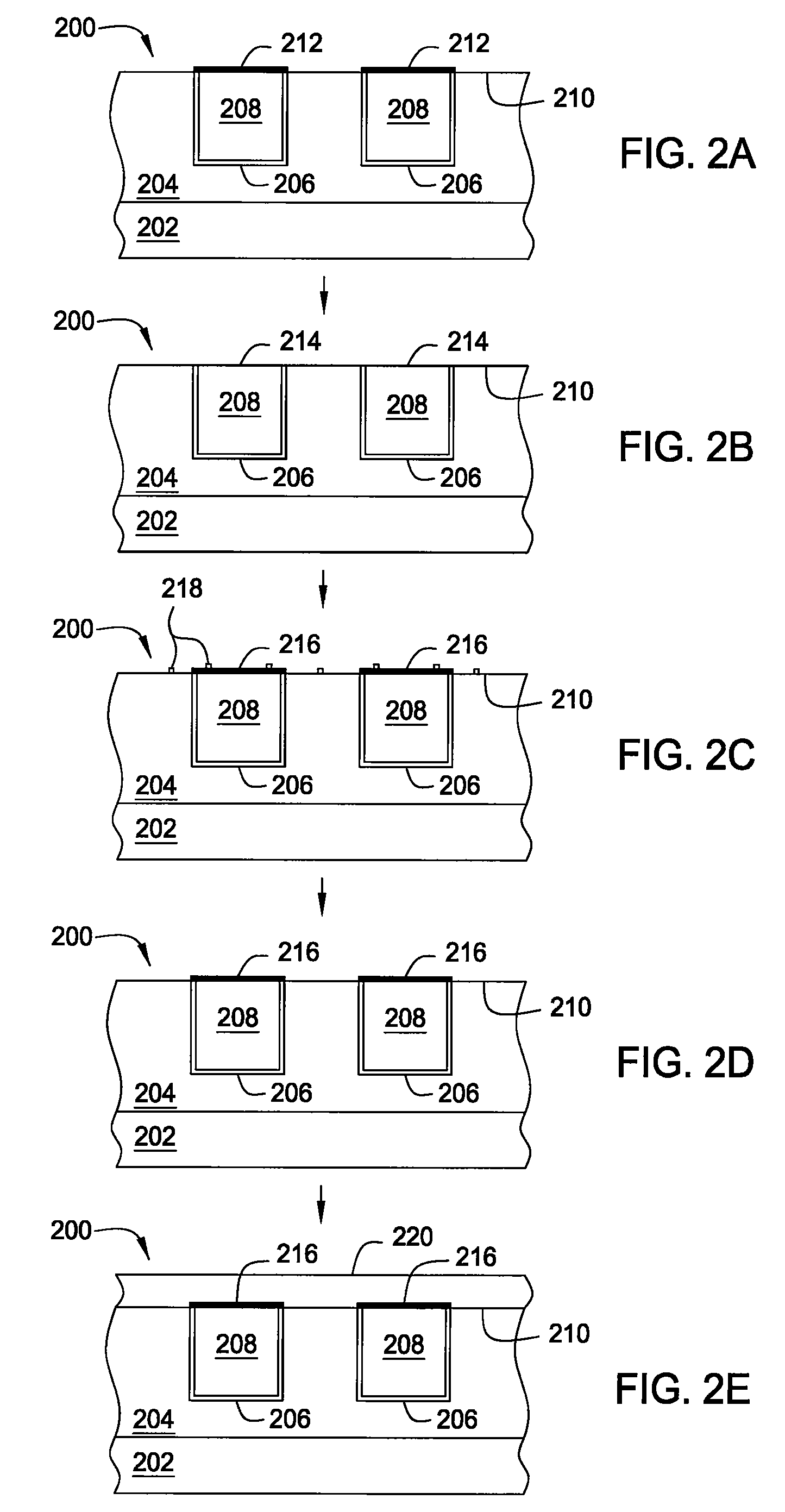
[0025]FIG. 1 depicts a flow chart illustrating process 100 according to an embodiment of the invention. Process 100 may be used to clean and cap a copper contact surface on a substrate post a polishing process. In one embodiment, steps 110-140 of process 100 may be used on substrate 200, depicted in FIGS. 2A-2E. Process 100 includes exposing a substrate to pre-treatment process (step 110), depositing a...


PUM

PropertyMeasurementUnit
Temperatureaaaaaaaaaa
Timeaaaaaaaaaa

Abstract

Embodiments of the invention provide processes to selectively form a cobalt layer on a copper surface over exposed dielectric surfaces. In one embodiment, a method for capping a copper surface on a substrate is provided which includes positioning a substrate within a processing chamber, wherein the substrate contains a contaminated copper surface and a dielectric surface, exposing the contaminated copper surface to a reducing agent while forming a copper surface during a pre-treatment process, exposing the substrate to a cobalt precursor gas to selectively form a cobalt capping layer over the copper surface while leaving exposed the dielectric surface during a vapor deposition process, and depositing a dielectric barrier layer over the cobalt capping layer and the dielectric surface. In another embodiment, a deposition-treatment cycle includes performing the vapor deposition process and subsequently a post-treatment process, which deposition-treatment cycle may be repeated to form multiple cobalt capping layers.

Description

BACKGROUND OF THE INVENTION[0001]1. Field of the Invention[0002]Embodiments of the invention generally relate to a metallization process for manufacturing semiconductor devices, more particularly, embodiments relate to preventing copper dewetting by depositing cobalt materials on a substrate.[0003]2. Description of the Related Art[0004]Copper is the current metal of choice for use in multilevel metallization processes that are crucial to semiconductor device manufacturing. The multilevel interconnects that drive the manufacturing processes require planarization of high aspect ratio apertures including contacts, vias, lines, and other features. Filling the features without creating voids or deforming the feature geometry is more difficult when the features have higher aspect ratios. Reliable formation of interconnects is also more difficult as manufacturers strive to increase circuit density and quality.[0005]As the use of copper has permeated the marketplace because of its relative ...

Claims


Application Information

Patent Timeline
IPC IPC(8): B05D3/04B05D5/12C23C16/44
CPCH01L21/02074H01L21/2855H01L21/28556H01L21/76849H01L21/02068H01L21/76883C23C16/0218C23C16/16C23C16/18H01L21/76862H01L21/28562H01L21/7685H01L21/324C23C16/45542C23C16/50C23C16/0245C23C16/4554
Inventor YU, SANG-HOMORAES, KEVINGANGULI, SESHADRICHUNG, HUAPHAN, SEE-ENG
Owner APPLIED MATERIALS INC
Why Eureka
Try Eureka