
Antenna device and wireless communication apparatus

a wireless communication apparatus and antenna device technology, applied in the direction of resonant antennas, elongated active element feeds, independent non-interacting antenna combinations, etc., can solve the problems of difficult to meet the expectations described, the mounting area of radiation electrodes becomes extremely small, and the antenna unit's characteristics are degraded, so as to reduce bandwidth, reduce the effect of harmonic frequency and simple structur

Inactive Publication Date: 2009-11-05
MURATA MFG CO LTD
View PDF17 Cites 36 Cited by
  • Summary
  • Abstract
  • Description
  • Claims
  • Application Information

AI Technical Summary

Benefits of technology

[0021]The embodiments disclosed herein provide solutions to the problems described above. Disclosed is a compact and low-cost antenna device in which no interference occurs even if many antenna units corresponding to various systems are mounted close together in a small area. Also disclosed is a wireless communication apparatus including the antenna device.

Problems solved by technology

However, when a plurality of antenna units are mounted, if antenna units having close fundamental frequencies are located close together or if a first antenna unit and a second antenna unit having a fundamental frequency close to a harmonic frequency in the first antenna unit are located close together, interference may occur and cause degradation in characteristics of these antenna units.
At the same time, as the size of mobile phones shrinks, a mounting area for mounting radiation electrodes becomes extremely small.
However, with the foregoing known techniques, it is difficult to meet the expectation described above.
Therefore, if a number of such antennas are arranged close together, currents flowing through bases of antennas having close fundamental frequencies may cause very strong coupling of magnetic fields, and interference may occur between these antennas.
This may result in deterioration in isolation between antennas and degradation of antenna gain.
This not only hinders a size reduction in the direction of thickness of the mobile phone, but also causes a problem of strength of component mounting.
Thus, since fundamental waves and harmonics cannot be independently controlled, the harmonic frequency may overlap with the fundamental frequency of another system, and thus, mutual interference may occur.
Thus, with the techniques described in Patent Documents 1 and 2, it is difficult to simultaneously solve the problem of interference between fundamental frequencies and the problem of interference between a harmonic frequency and a fundamental frequency.
Even if a number of these antenna devices are mounted, it is not possible to meet the expectation described above.
This means that costs involved in forming a radiation electrode and the like on each substrate are multiplied by the number of antenna units.
This makes the process more complicated.
However, depending on the size of the antenna mounting area, the distance between the first antenna unit and the second antenna unit may not be sufficient.

Method used


Image

  • Antenna device and wireless communication apparatus
  • Antenna device and wireless communication apparatus
  • Antenna device and wireless communication apparatus

Examples


first embodiment

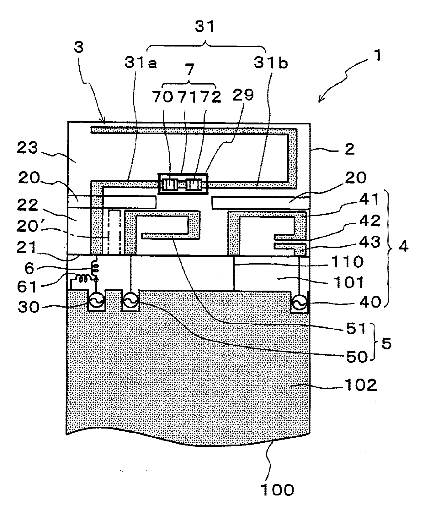
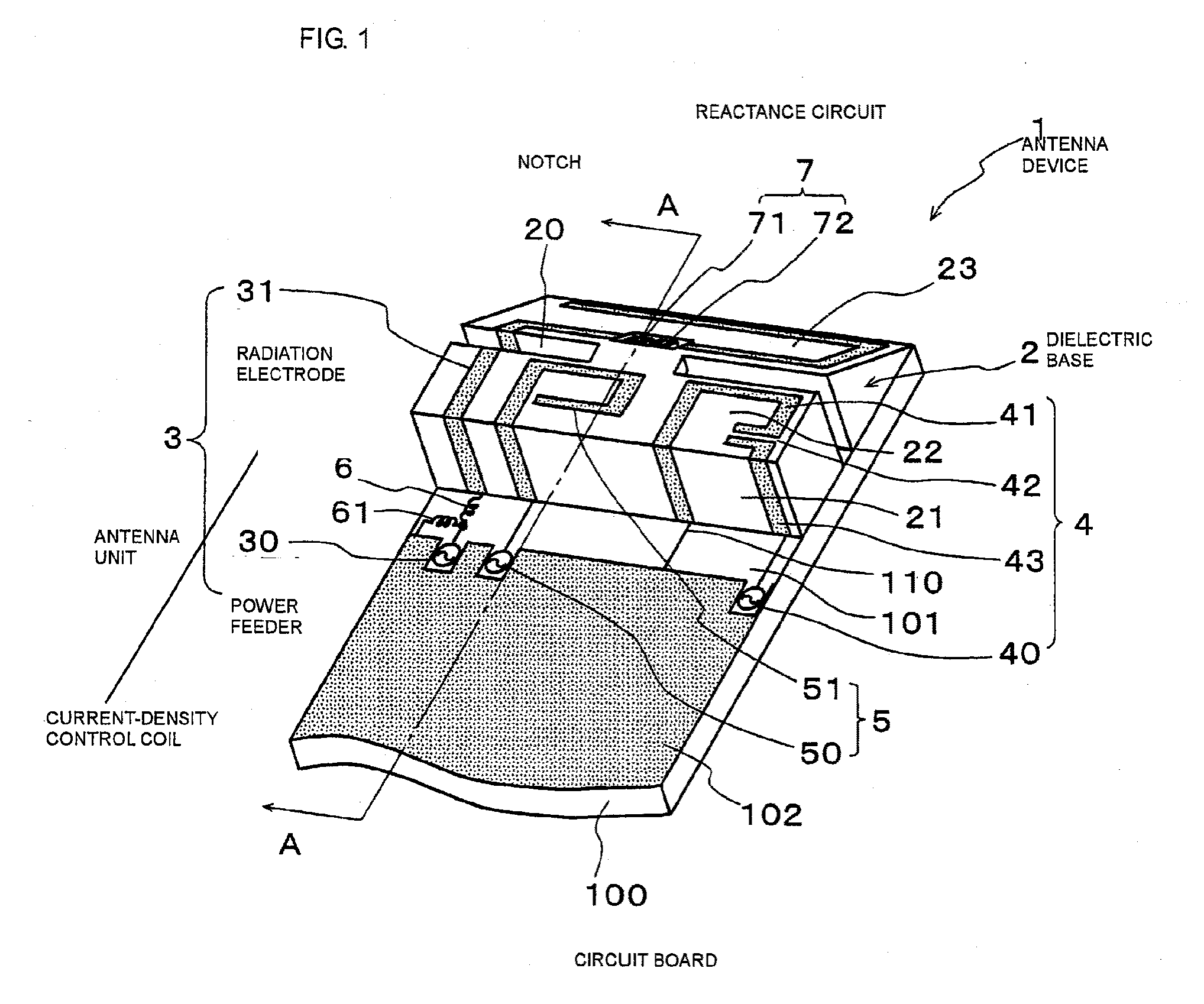
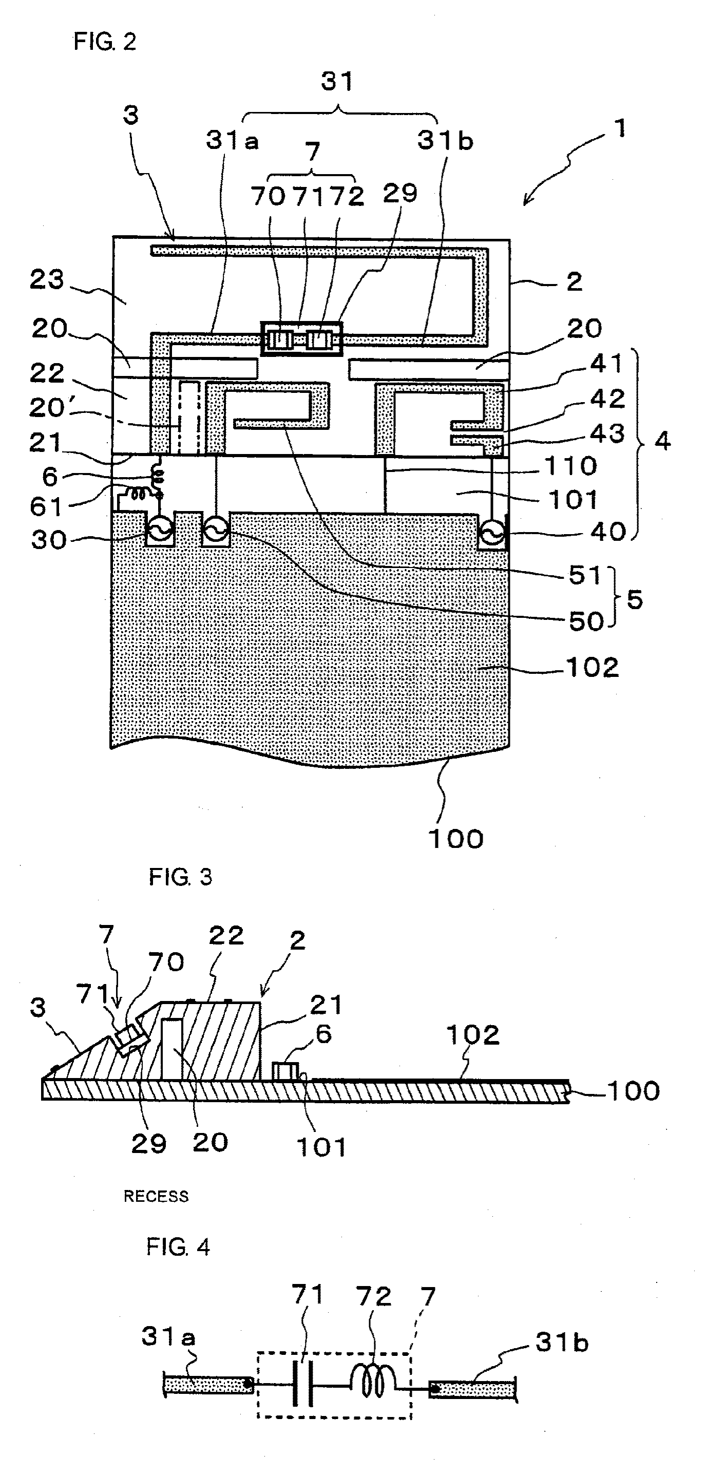
[0101]FIG. 1 is a perspective view of an antenna device according to a first embodiment. FIG. 2 is a plan view of the antenna device. FIG. 3 is a cross section as viewed in the direction of arrow A-A of FIG. 1.

[0102]As illustrated in FIG. 1, an antenna device 1 of the present embodiment is a multisystem antenna device for being included in a wireless communication apparatus, such as a mobile phone or a PC card, and mounted on a circuit board 100 to be included in the wireless communication apparatus.

[0103]Specifically, the antenna device 1 is formed by providing a single dielectric base 2 on a non-ground region 101, which serves as an antenna mounting area, and mounting three antenna units 3, 4, and 5 on the dielectric base 2.

[0104]The dielectric base 2 is integrally molded with dielectric material, positioned near an extremity of the antenna device 1 (i.e., on the upper end as seen in FIG. 1), and secured to the non-ground region 101.

[0105]Specifically, the dielectric base 2 has a ...

second embodiment

[0148]Next, a second embodiment will be described.

[0149]FIG. 13 is a plan view of an antenna device according to the second embodiment. FIG. 14 is a circuit diagram illustrating the reactance circuit 7 of the second embodiment.

[0150]The antenna device of the present embodiment is different from that of the first embodiment in that a branched radiation electrode 32a is added to the antenna unit 3.

[0151]Specifically, as illustrated in FIG. 13, the branched radiation electrode 32a is horizontally formed on the inclined surface 23 of the dielectric base 2 and connected to the reactance circuit 7. Then, the reactance circuit 7 is configured to allow the branched radiation electrode 32a to be connected to the base portion 31a of the radiation electrode 31.

[0152]Specifically, as illustrated in FIG. 14, two series resonant circuits reversely oriented with respect to each other, each series resonant circuit including the capacitor 71 and the inductor 72, are connected to each other. Then, an...

third embodiment

[0160]Next, a third embodiment will be described.

[0161]FIG. 17 is a plan view of an antenna device according to the third embodiment of the present invention. FIG. 18 is a partial enlarged cross-sectional view of the antenna device.

[0162]The present embodiment is different from the second embodiment in that the branched radiation electrode 32a is disposed not on the inclined surface 23 of the dielectric base 2, but on any exposed surface.

[0163]Specifically, as illustrated in FIG. 17 and FIG. 18, the branched radiation electrode 32a is horizontally disposed on an exposed surface 24 which is an exposed surface of the dielectric base 2 and on which the radiation electrodes 31, 41, and 51 of the antenna units 3, 4, and 5, respectively, are not disposed. Then, a conductive path 121 is connected to the open end c (see FIG. 16) of the reactance circuit 7, extends from the bottom of the recess 29 to the exposed surface 24 which is an inner surface of the notch 20, and then is connected to a...


PUM


Abstract

A compact and low-cost antenna device in which no interference occurs even when many antenna units corresponding to various systems are mounted close together in a small area, and a wireless communication apparatus including the antenna device. An antenna device includes plural antenna units mounted on a single dielectric base. A first antenna unit having a lowest fundamental frequency is disposed at a left end of a non-ground region, a second antenna unit having a highest fundamental frequency of the plurality of the antenna units is disposed at a right end of the non-ground region, and a third antenna unit having a fundamental frequency between those of the first antenna unit and the second antenna unit is disposed between the first and second antenna units. A current-density control coil is connected between a first radiation electrode and a power feeder of the first antenna unit, while a reactance circuit is disposed in the middle of the first radiation electrode. Notches may be disposed between the first radiation electrode and a second radiation electrode and between the first radiation electrode and a third radiation electrode.

Description

CROSS-REFERENCE TO RELATED APPLICATIONS[0001]This is a continuation under 35 U.S.C. §111(a) of PCT / JP2007 / 071427 filed Nov. 2, 2007, and claims priority of JP2007-010139 filed Jan. 19, 2007, both incorporated by reference.BACKGROUND[0002]1. Technical Field[0003]The present invention relates to frequency-adjustable antenna devices, and particularly to an antenna device and a wireless communication apparatus for multisystem communication.[0004]2. Background Art[0005]Examples of known techniques relating to antenna devices of this type are described in Patent Document 1 and Patent Document 2.[0006]Patent Document 1 describes a frequency variable antenna having a loop-shaped radiation electrode that performs a monopole antenna operation. The frequency variable antenna is provided with a frequency variable circuit in the middle of the radiation electrode. Thus, by externally applying a voltage to the frequency variable circuit to vary a reactance component of the frequency variable circu...

Claims


Application Information

Patent Timeline
Patent Type & Authority Applications(United States)
IPC IPC(8): H01Q1/38H01Q9/00H01Q1/52H01Q21/30
CPCH01Q1/243H01Q1/38H01Q9/145H01Q5/40H01Q21/28H01Q23/00H01Q1/523H01Q9/42
Inventor ISHIZUKA, KENICHIKAWAHATA, KAZUNARITSUBAKI, NOBUHITOFUJIEDA, SHIGEYUKINAKANO, SHINICHI
Owner MURATA MFG CO LTD
Learn More