Manufacturing method of thin film transistor array substrate and liquid crystal display panel

a manufacturing method and technology of liquid crystal display panels, applied in the field of manufacturing thin film transistor array substrates, can solve the problems of poor photoelectric effect and measurement distortion of p-i-n photo sensors manufactured through the ltps process, and achieve the effect of enhancing photo sensing efficiency and enlarged photo sensing area

Active Publication Date: 2009-11-19
AU OPTRONICS CORP
View PDF6 Cites 19 Cited by
  • Summary
  • Abstract
  • Description
  • Claims
  • Application Information

AI Technical Summary

Benefits of technology

[0007]The present invention relates to a manufacturing method of a thin film transistor array substrate incorporating a photo sensor which has an enlarged photo sensing area and enhanced photo sensing efficiency.
[0008]The present invention further relates to a manufacturing method of a thin film transistor array substrate incorporating a photo sensor. The method can effectively prevent backlight source from irradiating the photo sensor such that the photo sensor has more accurate measurement results.
[0019]In one embodiment of the present invention, to prevent the problem of over etching on the lower inter-layer dielectric layer when the photo sensitive dielectric layer is formed, a material of the inter-layer dielectric layer is preferably chosen according to a material of the photo sensitive dielectric layer. The inter-layer dielectric layer may also be formed with an etching barrier layer and a lower dielectric layer so as to increase an etching selectivity ratio.
[0024]In the manufacturing process of a thin film transistor array substrate incorporating manufacture of a photo sensor, a photo sensitive dielectric layer is formed between a transparent conductive layer and a metal electrode to sense incident light. At one side of the photo sensitive dielectric layer is the transparent conductive layer so incident light can directly irradiate the photo sensitive dielectric layer through the transparent conductive layer and thus sensing area of the photo sensor is significantly increased and so is the photo sensing efficiency. In addition, at the other side of the photo sensitive dielectric layer may be a metal electrode so backlight source can be prevented from directly irradiating the photo sensitive dielectric layer and thus possible influence by noise can be avoided.

Problems solved by technology

However, due to limitation of the process, the p-i-n photo sensor manufactured through the LTPS process has a problem of poor photoelectric effect because of insufficient thickness of the poly-silicon film and lower sensitivity.
In addition, light from a backlight source directly irradiates the p-i-n photo sensor through the glass substrate and thereby affects the photo sensing characteristics of the p-i-n photo sensor and reduces a signal to noise ratio (SNR) of a photo sensing signal, causing distortion of measurement results.

Method used


Image

  • Manufacturing method of thin film transistor array substrate and liquid crystal display panel
  • Manufacturing method of thin film transistor array substrate and liquid crystal display panel
  • Manufacturing method of thin film transistor array substrate and liquid crystal display panel

Examples


Embodiment Construction

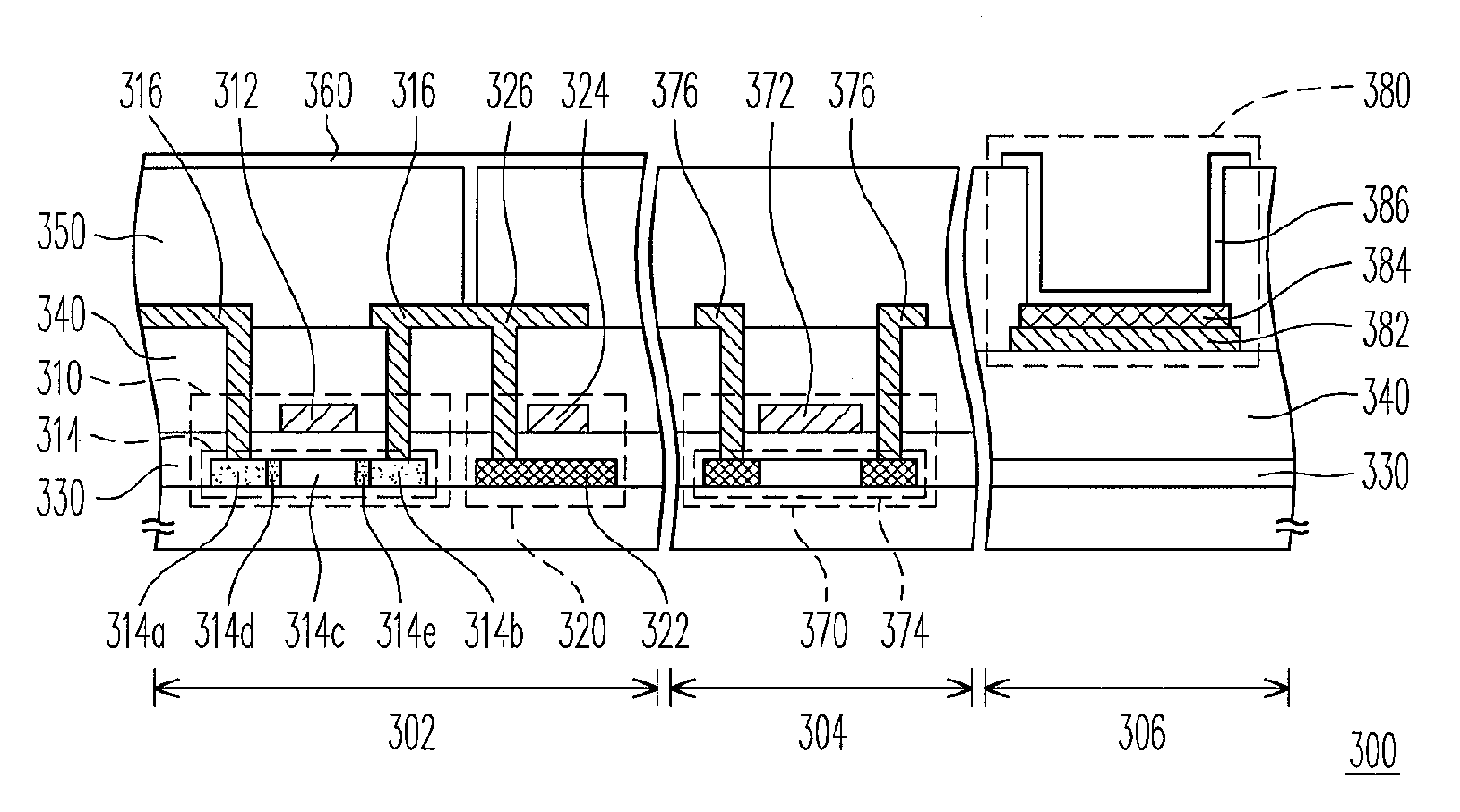
[0034]FIG. 1 illustrates a layout of a liquid crystal display panel incorporating a photo sensor according to an embodiment of the present invention. As shown in FIG. 1, a liquid crystal display panel 100 has at least a display region 110, a peripheral circuit region 120 in the periphery of the display region 110, and a sensing region 130. The display region 110 has a plurality of pixel units to display a frame. Possible driving elements such as a scan driver or a data driver are disposed in the peripheral circuit region 120. The sensing region 130 is used for disposing a photo sensor to detect intensity of ambient light and accordingly adjust brightness of a backlight source of the display so as to achieve power conservation. Meanwhile, by detecting intensity of ambient light, brightness and contrast of the liquid crystal display panel may be automatically adjusted so that not only fatigue of the eye resulted from high brightness and reflection can be reduced but energy consumption...


PUM


Abstract

A manufacturing method of a thin film transistor array substrate incorporating the manufacture of a photo-sensor is provided. In the manufacturing method, a photo-sensing dielectric layer is formed between a transparent conductive layer and a metal electrode for detecting ambient light. Since the transparent conductive layer is adopted as an electrode, the ambient light can pass through the transparent conductive layer and get incident light into the photo-sensing dielectric layer. Therefore, the sensing area of the photo-sensor can be enlarged and the photo-sensing efficiency is improved. In addition, the other side of the photo sensitive dielectric layer may be a metal electrode. The metal electrode can block the backlight from getting incident into the photo-sensing dielectric layer and thus reduce the background noise. A manufacturing method of a liquid crystal display panel adopting the aforementioned thin film transistor array substrate is also provided.

Description

CROSS-REFERENCE TO RELATED APPLICATION[0001]This application claims the priority benefit of Taiwan applications serial no. 97118209, filed May 16, 2008 and no. 97151836, filed Dec. 31, 2008. The entirety of each of the above-mentioned patent applications is hereby incorporated by reference herein and made a part of specification.BACKGROUND OF THE INVENTION[0002]1. Field of the Invention[0003]The present invention relates to a method of manufacturing a thin film transistor array substrate, and more particularly, to a method of manufacturing a thin film transistor array substrate incorporating a photo sensor.[0004]2. Description of Related Art[0005]With the popularity of liquid crystal and plasma displays, flat panel displays have become the so-called “multimedia board” in addition to being used for displaying images. A new development focus of the current display technology is to integrate an ambient light sensing capability in the flat panel display, which mainly is to build a photo...

Claims


Application Information

Patent Timeline
Patent Type & Authority Applications(United States)
IPC IPC(8): H01L21/28
CPCG02F1/13318H04N21/42202G02F2201/58G09G3/3406G09G3/3611G09G2320/0626G09G2320/066G09G2330/021G09G2360/144H01L27/1214H01L31/103H01L31/105H04N5/58H04N5/66G02F1/136213H01L27/127
Inventor CHO, AN-THUNGPENG, CHIA-TIENHSU, YUAN-JUNSHIH, CHING-CHIEHWENG, CHIEN-SENLIN, KUN-CHIHTSEUG, HANG-WEICHUANG, MING-HUANG
Owner AU OPTRONICS CORP
Why Eureka
Try Eureka