Methods For Forming Anti-Reflection Structures For CMOS Image Sensors

Active Publication Date: 2009-11-19
SMARTSENS TECH (HK) CO LTD
View PDF64 Cites 82 Cited by
  • Summary
  • Abstract
  • Description
  • Claims
  • Application Information

AI Technical Summary

Benefits of technology

[0011]In the present invention, protuberances, having vertical and lateral dimensions less than the wavelength range of lights detectable by a photodiode, are formed at an optical interface between two layers having different refractive indices and located in the optical path of lights impinging on the photodiode. The protuberances may be formed by employing self-assembling block copolymers that form an array of sublithographic features of a first polymeric block component within a matrix of a second polymeric bl

Problems solved by technology

Despite such structural modifications introduced into a pixel structure, loss of light due to reflection in the op

Method used


Image

  • Methods For Forming Anti-Reflection Structures For CMOS Image Sensors
  • Methods For Forming Anti-Reflection Structures For CMOS Image Sensors
  • Methods For Forming Anti-Reflection Structures For CMOS Image Sensors

Examples


second embodiment

[0124]Referring to FIG. 9, an exemplary M2 level metal interconnect structure according to the present invention is shown. The exemplary M2 level metal interconnect structure may be incorporated into the second exemplary semiconductor structure of FIG. 8. The exemplary M2 level metal interconnect structure comprises second metal line (M2) level dielectric layer 40, a V1 via 46, M2 lines 48, and an M2 level dielectric cap layer 42. The V1 via and M2 lines comprise a conductive metal such as W, Cu, Al, etc. The M2 level dielectric layer 40 comprises a dielectric material such as doped or undoped silicon oxide, organosilicate glass, SiCOH dielectric material, a spin-on dielectric material such as SiLK™, etc. The thickness of the M2 level dielectric cap layer 42 may be from about 100 nm to about 2,000 nm, and typically from about 150 nm to about 600 nm, although lesser and greater thicknesses are contemplated herein also. The M2 level dielectric cap layer 42 comprises another dielectric...

first embodiment

[0127]Referring to FIG. 12, the second exemplary semiconductor structure is annealed in the same manner as in the The anneal induces self-aligned separation of a first polymeric block component, which constitutes the polymeric block matrix 112, and a second polymeric block component, which constitutes the cylindrical polymeric blocks 111. The first polymeric block component and the second polymeric block component are immiscible with each other, and thus, separate into the two distinct types of structures, i.e., the polymeric block matrix 112 and the cylindrical polymeric blocks 111 upon the anneal. The polymeric block matrix 112 may have a horizontal cross-sectional shape including an array of cavities in the shape of a polygon, such as a hexagon, or a circle depending on the viscosity and composition of the components of the block copolymer layer 110. Typically, the polymeric block matrix 112 are arranged in a regular periodic array, i.e., in an array structure having a two dimen...

third embodiment

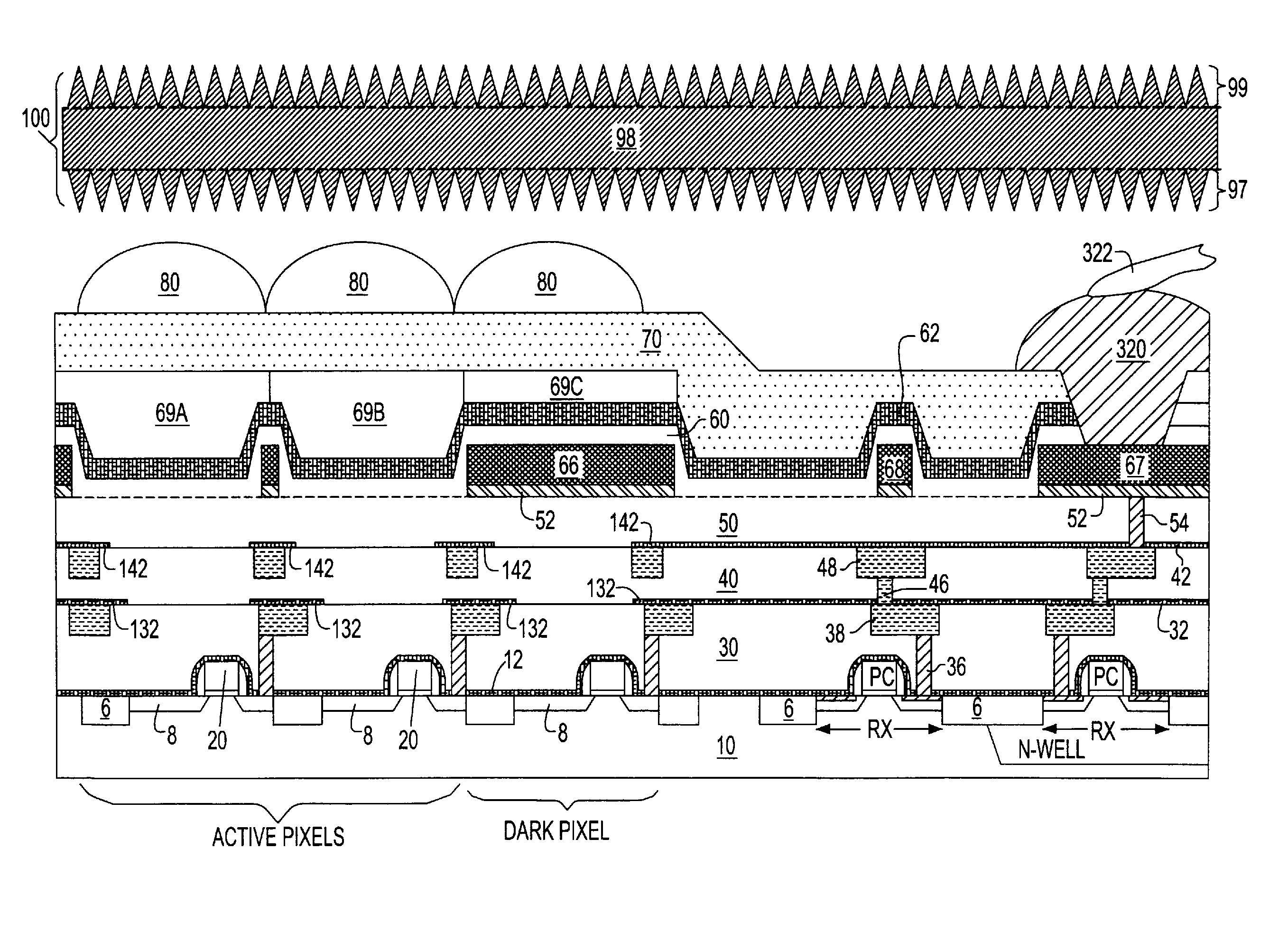
[0135]Referring to FIG. 16, a third exemplary semiconductor structure according to the present invention comprises an exemplary device, which is a portion of a CMOS image sensor pixel. The exemplary device includes a semiconductor substrate 108 and a gate structure for a transfer gate transistor. The semiconductor substrate 108 comprises a p+ doped semiconductor layer 110, a p− doped semiconductor layer 112, and a shallow trench isolation structure 120. The semiconductor substrate 108 further comprises a photodiode and a surface pinning layer 134 having a p-type doping. The photodiode comprises an n-type charge collection well 130 located beneath the surface pinning layer 134 and a p-type well 132, which is a portion of the p− doped semiconductor layer 112 and vertically abuts the p+ doped semiconductor layer 110. The transfer gate transistor is integrally formed with the photodiode (130, 132) such that the n-type charge collection well 130, which comprises an n+ doped semiconductor...


PUM


Abstract

Protuberances, having vertical and lateral dimensions less than the wavelength range of lights detectable by a photodiode, are formed at an optical interface between two layers having different refractive indices. The protuberances may be formed by employing self-assembling block copolymers that form an array of sublithographic features of a first polymeric block component within a matrix of a second polymeric block component. The pattern of the polymeric block component is transferred into a first optical layer to form an array of nanoscale protuberances. Alternately, conventional lithography may be employed to form protuberances having dimensions less than the wavelength of light. A second optical layer is formed directly on the protuberances of the first optical layer. The interface between the first and second optical layers has a graded refractive index, and provides high transmission of light with little reflection.

Description

RELATED APPLICATIONS[0001]The present application is related to a co-pending U.S. patent application Ser. No. ______ (attorney docket: BUR920070255US1) concurrently filed with the present application, which is incorporated herein by reference.FIELD OF THE INVENTION[0002]The present invention relates to semiconductor structures, and particularly to methods of manufacturing anti-reflection structures for complementary metal-oxide-semiconductor image sensors.BACKGROUND OF THE INVENTION[0003]An image sensor converts a visual image to digital data that may be represented by a picture. The image sensor comprises an array of pixels, which are unit devices for the conversion of the visual image into digital data. Digital cameras and optical imaging devices employ an image sensor. Image sensors include charge-coupled devices (CCDs) or complementary metal oxide semiconductor (CMOS) image sensors.[0004]While CMOS image sensors have been more recently developed compared to the CCDs, CMOS image ...

Claims


Application Information

Patent Timeline
IPC IPC(8): H01L31/0236H01L31/18
CPCH01L27/14618H01L27/14625H01L2924/3025H01L2224/73265H01L2224/48227H01L2224/48091H01L2224/32225H01L27/14689H01L27/14685H01L27/14627H01L27/14632H01L27/14645H01L2924/00014H01L2924/00
Inventor ADKISSON, JAMES W.ELLIS-MONAGHAN, JOHN J.GAMBINO, JEFFREY P.MUSANTE, CHARLES F.
Owner SMARTSENS TECH (HK) CO LTD
Why Eureka
Try Eureka