Light-emitting device, display apparatus, and electronic system

Active Publication Date: 2009-12-03
SEIKO EPSON CORP
View PDF2 Cites 25 Cited by
  • Summary
  • Abstract
  • Description
  • Claims
  • Application Information

AI Technical Summary

Benefits of technology

[0008]An advantage of some aspects of the invention is that it provides a light-emitting device with high emission efficiency, a rel

Problems solved by technology

The light-emitting device according to Patent Document 1, however, has insufficient emission efficiency beca

Method used


Image

  • Light-emitting device, display apparatus, and electronic system
  • Light-emitting device, display apparatus, and electronic system
  • Light-emitting device, display apparatus, and electronic system

Examples


first embodiment

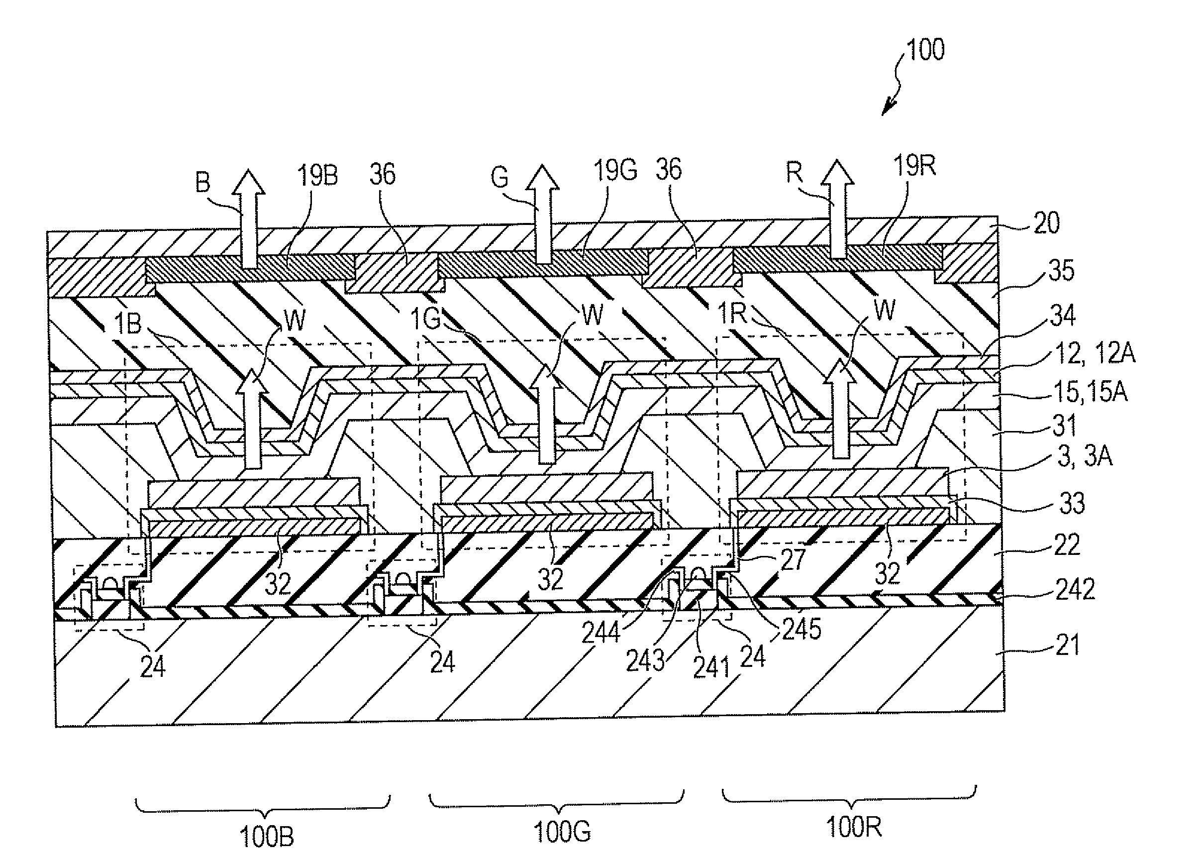
[0075]FIG. 1 is a schematic diagram showing the longitudinal section of a light-emitting device according to a first embodiment of the invention. For illustration purposes, the top of FIG. 1 is referred to as “top”, whereas the bottom of FIG. 1 is referred to as “bottom”.

[0076]A light-emitting device (EL device) 1 shown in FIG. 1 emits red (R) light, green (G) light, and blue (B) light to provide white light.

[0077]The light-emitting device 1 is formed by stacking an anode 3, a hole-injecting layer 4, a hole-transporting layer 5, a red light-emitting layer (first light-emitting layer) 6, an intermediate layer 7, a blue light-emitting layer (second light-emitting layer) 8, a green light-emitting layer (third light-emitting layer) 9, an electron-transporting layer 10, an electron-injecting layer 11, and a cathode 12 in the above order.

[0078]In other words, the light-emitting device 1 includes a laminate 15 formed between the two electrodes (the anode 3 and the cathode 12) by stacking t...

second embodiment

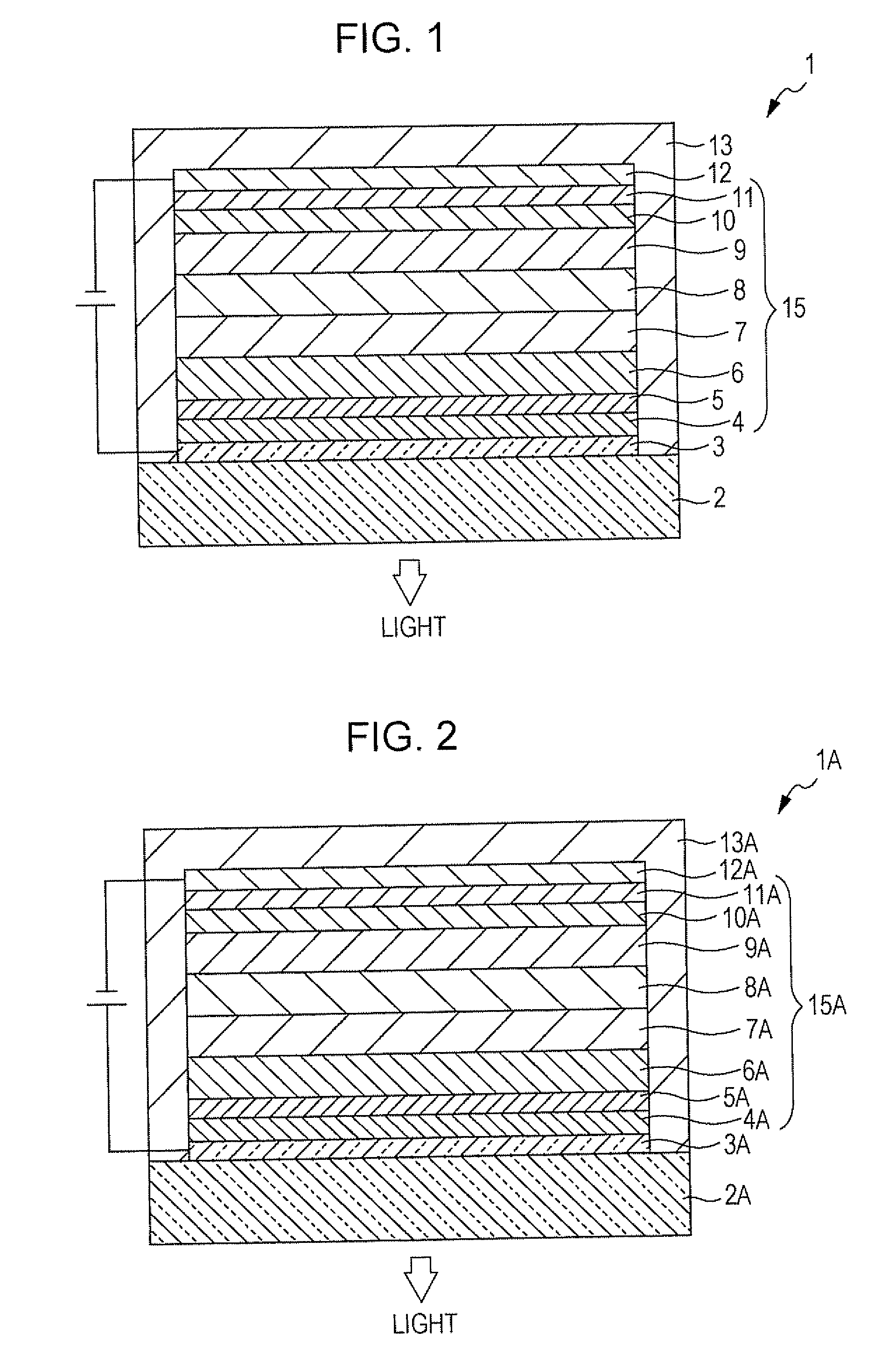
[0185]FIG. 2 is a schematic diagram showing the longitudinal section of a light-emitting device according to a second embodiment of the invention. For illustration purposes, the top of FIG. 2 is referred to as “top”, whereas the bottom of FIG. 2 is referred to as “bottom”.

[0186]A light-emitting device (EL device) 1A shown in FIG. 2 emits red (R) light, green (G) light, and blue (B) light to provide white light.

[0187]The light-emitting device 1A is formed by stacking an anode 3A, a hole-injecting layer 4A, a hole-transporting layer 5A, a red light-emitting layer (first light-emitting layer) 6A, an intermediate layer 7A, a blue light-emitting layer (second light-emitting layer) BA, a green light-emitting layer (third light-emitting layer) 9A, an electron-transporting layer 10A, an electron-injecting layer 11A, and a cathode 12A in the above order.

[0188]In other words, the light-emitting device 1A includes a laminate 15A formed between the two electrodes (the anode 3A and the cathode 1...

example 1

[0363](1) First, a transparent glass substrate with an average thickness of 0.5 mm was prepared. Next, an ITO electrode (anode) with an average thickness of 50 nm was formed on the substrate by sputtering.

[0364]The substrate was subjected to ultrasonic cleaning in acetone and then in 2-propanol and was subjected to oxygen plasma treatment.

[0365](2) Next, a hole-injecting layer with an average thickness of 30 nm was formed on the ITO electrode by depositing LG101 (manufactured by LG Chem, Ltd.) through vacuum deposition.

[0366](3) Next, a hole-transporting layer with an average thickness of 20 nm was formed on the hole-injecting layer by depositing N,N′-bis(1-naphthyl)-N,N′-diphenyl-1,1′-biphenyl-4,4′-diamine (α-NPD), represented by chemical formula 6 above, through vacuum deposition.

[0367](4) Next, a red light-emitting layer (first light-emitting layer) with an average thickness of 10 nm was formed on the hole-transporting layer by depositing the constituent materials of the red ligh...


PUM


Abstract

A light-emitting device includes a cathode, an anode, a first light-emitting layer that is disposed between the cathode and the anode and that emits light of a first color, a second light-emitting layer that is disposed between the first light-emitting layer and the cathode and that emits light of a second color different from the first color, and an intermediate layer that is disposed between and in contact with the first light-emitting layer and the second light-emitting layer and that contains a first material and a second material different from the first material. The light-emitting device satisfies inequality (1):
LLA−LLB≧0.4 [eV]  (1)
wherein LLA [eV] is the energy level of the lowest unoccupied molecular orbital of the first material, and LLB [eV] is the energy level of the lowest unoccupied molecular orbital of the second material.

Description

BACKGROUND[0001]1. Technical Field[0002]The present invention relates to light-emitting devices, display apparatuses, and electronic systems.[0003]2. Related Art[0004]An organic electroluminescent (EL) device is a light-emitting device including at least one organic light-emitting layer between an anode and a cathode. In this type of light-emitting device, an electric field is applied between the anode and the cathode to inject electrons from the cathode into the light-emitting layer and holes from the anode into the light-emitting layer. The electrons and the holes then recombine together in the light-emitting layer to generate excitons. When the excitons return to the ground state, their energy is released in the form of light.[0005]One such light-emitting device includes two light-emitting layers, corresponding to red (R) and blue (B), that are stacked between the anode and the cathode so that the device can emit white light (for example, see JP-A-2007-287691 (Patent Document 1))...

Claims


Application Information

Patent Timeline
IPC IPC(8): H01L33/00
CPCH01L27/322H01L51/0058H01L2251/552H01L51/5036H01L51/006H10K59/38H10K85/626H10K85/633H10K50/125H10K2101/30H05B33/14H10K50/00
Inventor MITSUYA, MASAYUKI
Owner SEIKO EPSON CORP
Why Eureka
Try Eureka