Film with Transparent Conductive Layer, Flexible Functional Element and Flexible Dispersion-Type Electroluminescent Element, and Method for Producing the Same and Electronic Device by the Use Thereof

a technology of transparent conductive layer and flexible functional element, which is applied in the direction of discharge tube luminescnet screen, organic semiconductor device, synthetic resin layered product, etc., can solve the problems of easy cracking of microscopic cracks, high cost of color led, etc., to achieve sufficient keying durability, good click feeling of key operation, and excellent flexibility

Inactive Publication Date: 2009-12-10
SUMITOMO METAL MINING CO LTD
View PDF13 Cites 13 Cited by
  • Summary
  • Abstract
  • Description
  • Claims
  • Application Information

AI Technical Summary

Benefits of technology

[0030]According to the present invention, it is possible to inexpensively provide the film with the transparent conductive layer and various flexible functional elements such as flexible dispersion-type EL elements which are more excellent in flexibility than the conventional sputtering ITO films and various functional elements such as dispersion-type EL elements using those films.
[0031]Also when the above flexible dispersion-type EL element is applied to the keypad of the mobile phone, the element has the practically sufficient keying durability, and simultaneously it becomes possible to obtain the good click feeling of the key operation without giving a special structure and contrivance to the keypad.BEST MODE(S) FOR CARRYING OUT THE INVENTION
[0032]First, the flexible functional elements to which the film with the transparent conductive layer of the present invention can be applied include liquid crystal display elements, organic EL elements, electronic paper elements, and dispersion-type EL elements.
[0033]The above liquid crystal display element is a non-luminescent type electronic display element widely used for the displays of mobile phones, PDAS, PCs, and like, a simple matrix system and an active matrix system are available, and the active matrix system is more excellent in image quality and response speed. In its basic structure, the display is performed by sandwiching the liquid crystal with transparent electrodes and orienting the liquid crystal molecules by voltage driving, but the actual element is used by further laminating a color filter, a phase contrast film, and a polarization film in addition to the above transparent electrodes.
[0034]The above organic EL element is a self-luminescent element differently from the liquid display element and the high luminance is obtained by low voltage driving. Thus, this is expected as a display apparatus such as a display. Its structure is obtained by sequentially forming a positive hole injection layer (hole injection layer) composed of a conductive polymer such as a polythiophene derivative, an organic luminescent layer (a low molecular luminescent layer formed by vapor deposition and a high molecular luminescent layer formed by application), a cathode electrode layer (a metal layer of magnesium [Mg], calcium [Ca] or aluminium [Al] having a good electron injection property to the luminescent layer and a low work function) and a gas barrier coating layer (or a sealing treatment with a metal or a glass) on the transparent conductive layer as an anode electrode layer.
[0035]The above electronic paper element is a non-luminescent type electronic display element which does not emit the light by itself, comprises a memory effect that the display remains intact even if an electric power is turned off, and is expected as the display for character representation. Its display system can include an electrophoresis system in which colored particles are migrated in a liquid between the electrodes by electrophoresis, a twist ball system which pigmentizes by rotating the particles having a bicolor property in an electric field, e.g., a liquid crystal system in which the display is performed by sandwiching a cholesteric liquid crystal with transparent electrodes, a powder based system in which the display is performed by migrating colored particles (toner) or electric powder fluids (quick response liquid powder) in air, an electrochromic system in which the color is developed based on an electrochemical oxidation reduction action and an electrodeposition system in which the display is performed by color change depending on precipitation and dissolution of the metal by electrochemical oxidation and reduction.

Problems solved by technology

However, the dispersion-type EL element has been actively used in place of LED, since there are some issues in LED such that LED is emitted from a point source and a luminance in the keypad portion is uneven and an appearance thereof is poor; that although a white or blue luminescent color is generally popular, such a color requires a high cost in LED; and that LED requires a higher electric power consumption than the dispersion-type EL element.
However, there is a problem in the above sputtering ITO layer that microscopic cracks (cracks) easily occur therein since it is a thin film of the inorganic component and extremely fragile.
The PET film is widely used for a base film of the above sputtering ITO film, but when its thickness is less than 50 μm, the flexibility of the base film is too high, and the cracks easily occur in the sputtering ITO layer during handling to remarkably impair a conductivity of the film.
In this case, however, the conductivity and the flexibility can not be balanced in the sputtering ITO layer when the support film is delaminated and removed, since the flexibility of the sputtering ITO layer itself is poor.
Also, at present a soft base film, such as a urethane film, is not put to practical use even if its film thickness is 75 μm or more, for the cracks easily occur when the sputtering ITO layer is formed.
Also the base film of the flexible material can not be used.
Thus, when the element is applied to the above keypad, the keying durability is not sufficient yet and the click feeling is not sufficiently good.
However, in the method for forming the transparent conductive layer by these conventional coating methods, in order to obtain the property which is excellent in transparency and conductivity, there is no choice but to set a rolling pressure high.
However, in this case, when the thickness of the base film is made thin (e.g., 25 μm or less, particularly 9 μm or less), defects such as a distortion of the base film and an occurrence of the creases tend to occur and as a result, there is such problems that the productivity is reduced and yields of products worsen.
Therefore, there has been a limitation in industrial mass production such that in order to prevent them, the base film having the thickness of more than 25 μm (e.g., about 50 μm) is used.
Thus, even in the above method for forming the transparent conductive layer by the conventional coating method, since the base film used is still thick, it has not been possible to sufficiently respond to the flexibility and thinning of the EL element required for the key input parts (keypads).

Method used


Image

  • Film with Transparent Conductive Layer, Flexible Functional Element and Flexible Dispersion-Type Electroluminescent Element, and Method for Producing the Same and Electronic Device by the Use Thereof
  • Film with Transparent Conductive Layer, Flexible Functional Element and Flexible Dispersion-Type Electroluminescent Element, and Method for Producing the Same and Electronic Device by the Use Thereof

Examples


example 1

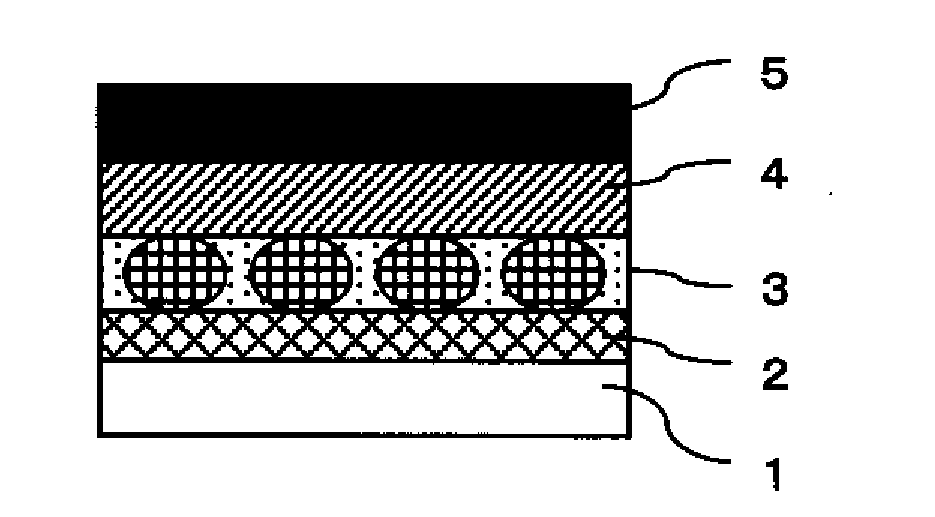
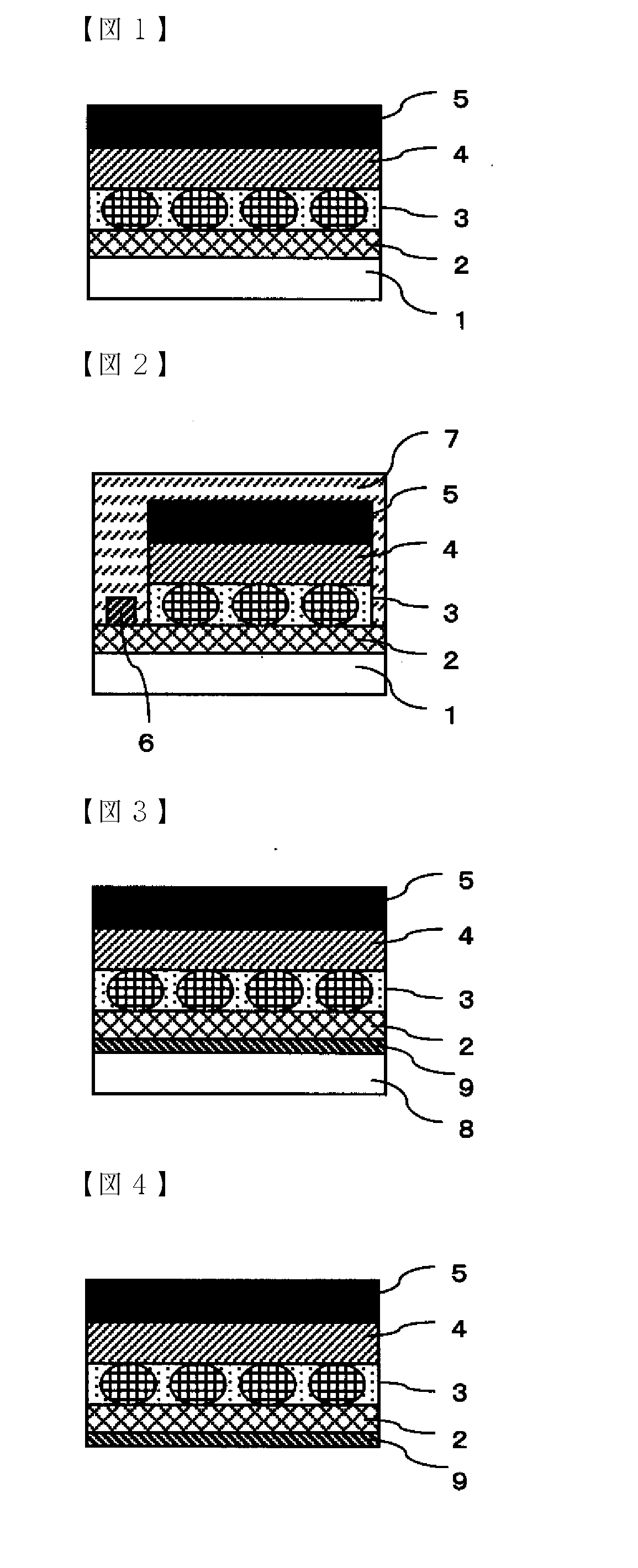
[0084]36 g of granular ITO microparticles having an average particle diameter of 0.03 μm (brand name: SUFP-HX made by Sumitomo Metal Mining Co., Ltd.) were mixed with 24 g of methyl isobutyl ketone (MIBK) and 36 g of cyclohexanone as the solvents, a dispersion treatment was given thereto, and subsequently 3.8 g of urethane acrylate based ultraviolet light curable resin binder and 0.2 g of a photo initiator (Dalocure 1173) were added and stirred well to yield a coating liquid for forming a transparent conductive layer in which the ITO microparticles having the dispersed average particle diameter of 130 nm were dispersed.

[0085]First, prior to producing a film with a transparent conductive layer, a heating shrinkage treatment (150° C.×15 minutes, tension free) was given to a base film (PET: thickness of 6 μm) lined with a support film (PET: thickness of 75 μm) via a heat resistant silicone low adhesive layer. Subsequently, the coating liquid for forming the transparent conductive layer...

example 2

[0094]The flexible dispersion-type EL element according to Example 2 was obtained in the same way as in Example 1, except that the coating liquid for forming the transparent conductive layer was wire-bar-coated (wire diameter: 0.075 mm) to form the transparent conductive layer (film thickness: about 0.5 μm) composed of the ITO microparticles and the binder, which were densely filled on the base film lined with the support film, to yield the film with the transparent conductive layer according to Example 2, having the peel strength of 2.4 g / cm between the support film and the base film, the dimensional change rate (thermal shrinkage rate) of 0.05% upon heating, the visible light transmittance of 95.1%, the haze value of 1.4% and the surface resistivity of 1500Ω / □ (ohms per square).

[0095]In the process for producing the above flexible dispersion-type EL element, the base film could be easily delaminated at the interface with the support film. The peel strength between the support film...

example 3

[0096]The film with the transparent conductive layer according to Example 3, having the peel strength of 2.3 g / cm between the support film and the base film, the dimensional change rate (thermal shrinkage rate) of 0.06% upon heating, the visible light transmittance of 95.0%, the haze value of 1.6% and the surface resistivity of 1500Ω / □ (ohms per square) was obtained in the same way as in Example 2, except that the heating shrinkage treatment (150° C.×15 minutes, tension free) was given to the base film (PET: thickness of 12 μm) lined with the support film (PET: thickness of 125 μm) via the heat resistant silicone low adhesive layer. The flexible dispersion-type EL element according to Example 3 was obtained in the same way as in Example 2, except for using this film with the transparent conductive layer.

[0097]In the process for producing the above flexible dispersion-type EL element, the base film could be easily delaminated at the interface with the support film. The peel strength ...


PUM

PropertyMeasurementUnit
thicknessaaaaaaaaaa
thermal shrinkageaaaaaaaaaa
thicknessaaaaaaaaaa

Abstract

An object of the present invention is to provide various flexible functional elements such as a film with a transparent conductive layer which is excellent in flexibility, more specifically, a film with the transparent conductive layer formed on a thin and flexible base film, and a flexible functional element selected from any of a liquid crystal display element, an organic EL element, and an electronic paper element as well as a flexible dispersion-type EL element, using the film with the transparent conductive layer, and a method for producing the same.There is provided a film with a transparent conductive layer, the layer being formed on a base film by a coating method, characterized in that the base film side of the film with the transparent conductive layer is lined with a support film having a low adhesive layer separable at an interface with the base film, the base film having a thickness of 3 to 25 μm, and that the transparent conductive layer is composed mainly of conductive oxide microparticles and a binder matrix, and a compression treatment is given thereto.

Description

TECHNICAL FIELD[0001]The present invention relates to a transparent conductive film obtained by forming a transparent conductive layer composed mainly of conductive oxide microparticles and a binder matrix on an ultrathin base film; a flexible functional element which is selected from any of a liquid crystal display element, an organic electroluminescent element and a electronic paper element; a dispersion-type electroluminescent element; wherein these elements are obtained using the film with the transparent conductive layer; and further relates to a method for producing the above-mentioned conductive film and elements, and an electronic device by the use thereof, and particularly relates to a dispersion-type electroluminescent element applied as a luminescent element incorporated in a key input part of various devices such as mobile phones, and to an electronic device by the use of the electroluminescent element.BACKGROUND ART[0002]In recent years, in various displays including li...

Claims


Application Information

Patent Timeline
Patent Type & Authority Applications(United States)
IPC IPC(8): H01J1/62H05K1/00B32B29/04B29C63/02
CPCH01L51/5206H05B33/28H01L2251/5338H01L2227/326H10K50/81H10K71/80H10K59/1201H10K2102/311
Inventor MURAYAMA, YUKIYUKINOBU, MASAYA
Owner SUMITOMO METAL MINING CO LTD
Why Eureka
Try Eureka