Semiconductor device

a technology of semiconductors and devices, applied in the field of semiconductor design technology, can solve the problems of impedance value, electrical energy interference, capacitance between, etc., and achieve the effect of removing skew and removing skew

Inactive Publication Date: 2009-12-10
SK HYNIX INC
View PDF12 Cites 2 Cited by
  • Summary
  • Abstract
  • Description
  • Claims
  • Application Information

AI Technical Summary

Benefits of technology

[0027]As discussed above, the prior art device employs complicated circuits such as a DLL circuit in order to remove skew caused by crosstalk. On the contrary, the invention detects the type of transition of transmission signal on each transmission line and judges a signal transmission mode between adjacent transmission lines based on the detected signal and adjusts a delay of transmission signal depending on the signal transmission mode. That is, the invention adjusts a delay difference of transmission signals based on such a delay difference by signal transmission modes, thereby removing skew.

Problems solved by technology

Therefore, even when transmission lines are arranged in the air, there may also be capacitance between them.
When an alternate current of high frequency band flows onto a transmission line, electrical energy interference occurs due to the influence of capacitance between transmission lines, i.e., mutual capacitance, as the current goes toward a higher frequency band.
This mutual inductance causes magnetic energy interference that affects the inductance value of each transmission line, etc, which in turn affects the characteristic impedance value of each transmission line.
As metals are closed to each other, this phenomenon gives rise to interference with a signal and acts as an undesired parasitic effect.
In result, such difference in the transmission rates acts as a factor that impairs a timing margin.
Therefore, such devices require numerous control signals therein, thus making their circuits complicated and wider in area, together with much power consumption.

Method used


Image

  • Semiconductor device
  • Semiconductor device
  • Semiconductor device

Examples


Embodiment Construction

[0038]Hereinafter, preferred embodiments of the present invention will be described in detail with reference to the accompanying drawings, so that the invention can readily be practiced by those skilled in the art to which the invention pertains.

[0039]Typically, in logic circuits, a digital logic signal is identified as a logic high level or a logic low level, which is expressed as ‘1’ or ‘0’, respectively. In addition, it may further have a high impedance (HI-Z) state, etc., as further discussed below.

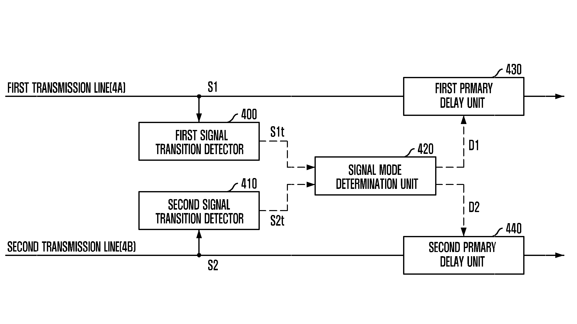
[0040]FIG. 3A is a block diagram showing the configuration of a semiconductor device in accordance with one embodiment of the invention. Referring to FIG. 3A, the semiconductor device of this embodiment includes a first transmission unit having first transmission line 4A, first signal transition detector 400 and first delay unit 430, and a second transmission unit includes second transmission line 4B, second signal transition detector 410 and second delay unit 440. The first and secon...


PUM


Abstract

A semiconductor device includes transmission lines for conveying signals and transition detectors, each of which checks whether a transmission signal on each of the plurality of transmission lines is transited. If the signal is transited, its transition shape is detected. A signal mode determining unit determines signal transmission modes between adjacent transmission lines in response to output signals from the plurality of transition detectors. Delay units are coupled to the respective transmission lines for adjusting transmission delays of the transmission signals depending on corresponding output signal from the signal mode determining units.

Description

CROSS-REFERENCE TO RELATED APPLICATION[0001]The present invention claims priority from Korean patent application number 10-2008-0052753, filed on Jun. 4, 2008, which is incorporated by reference in its entirety.BACKGROUND OF THE INVENTION[0002]The present invention relates to a semiconductor design technology; and more particularly, to a technology of removing crosstalk that may occur between transmission lines of the semiconductor device.[0003]In semiconductor devices, when a signal is transmitted via a transmission line, the signal may be affected by electromagnetic fields, which will be discussed in detail below.[0004]When a dielectric is between metals, there is capacitance between them. In general, a transmission line is made of metal and a dielectric is arranged between transmission lines, and thus, capacitance may exist between them. It is known that even air is a dielectric whose relative dielectric constant is ‘1’. Therefore, even when transmission lines are arranged in the...

Claims


Application Information

Patent Timeline
Patent Type & Authority Applications(United States)
IPC IPC(8): H01P9/00
CPCH03K5/131H03K5/135H03K5/1534H04L25/029H04B3/32H04L25/0272H04L25/0286H03K2005/00071G11C7/10G11C8/00
Inventor LEE, JI-WANGPARK, KUN-WOOKIM, YONG-JUSONG, HEE-WOONGOH, IC-SUKIM, HYUNG-SOOHWANG, TAE-JINCHOI, HAE-RANG
Owner SK HYNIX INC
Why Eureka
Try Eureka