Germanium-enriched silicon material for making solar cells

a silicon material and solar cell technology, applied in the direction of polycrystalline material growth, crystal growth process, crystal growth process, etc., can solve the problems of solar cell processing and handling, wafer breakage at wafer, degradation of cell properties, etc., to improve the control of intrinsic material strength, increase material strength, and increase compressive lattice strain

Inactive Publication Date: 2009-12-17
HIGHLAND MATERIALS INC
View PDF27 Cites 19 Cited by
  • Summary
  • Abstract
  • Description
  • Claims
  • Application Information

AI Technical Summary

Benefits of technology

[0042]The silicon material improvements of the present disclosure may derive from increased compressive lattice strain associated with substitutionally incorporating germanium atoms in the lattice structure of crystalline silicon. Such substitutional incorporation of germanium may compensate local tensile stresses associated with certain bulk defects in silicon wafers or solar cells and result in improved control of the intrinsic material strength.
[0043]Empirical results indicate that a silicon material with a germanium concentration in the range (50-200) ppmw demonstrates an increased material strength, where the best practical range depends on the material quality generated. Slightly higher germanium concentrations turn out to work better for mono-crystalline silicon, as compared to multi-crystalline silicon.

Problems solved by technology

Also carbon related and oxygen related defects in the wafer bulk can degrade cell properties, in particular when associated with metals.
In any case, since silicon is brittle at room temperature, there is the general problem of wafer breakage at wafer and solar cell processing and handling, including the manufacturing of modules out of solar cells.
Cracks may originate from, for example, handling-induced local damage on surfaces, in particular at edges and corners.

Method used


Image

  • Germanium-enriched silicon material for making solar cells
  • Germanium-enriched silicon material for making solar cells
  • Germanium-enriched silicon material for making solar cells

Examples


Embodiment Construction

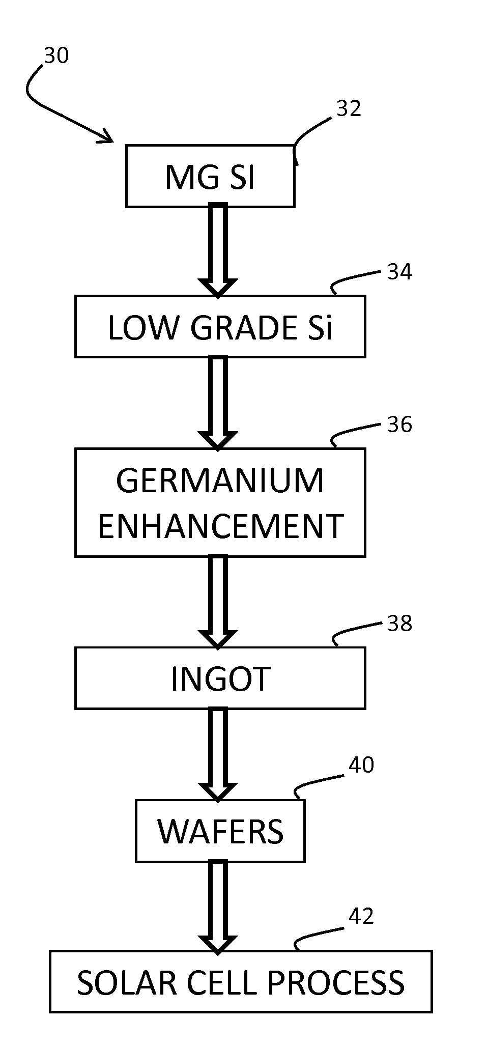
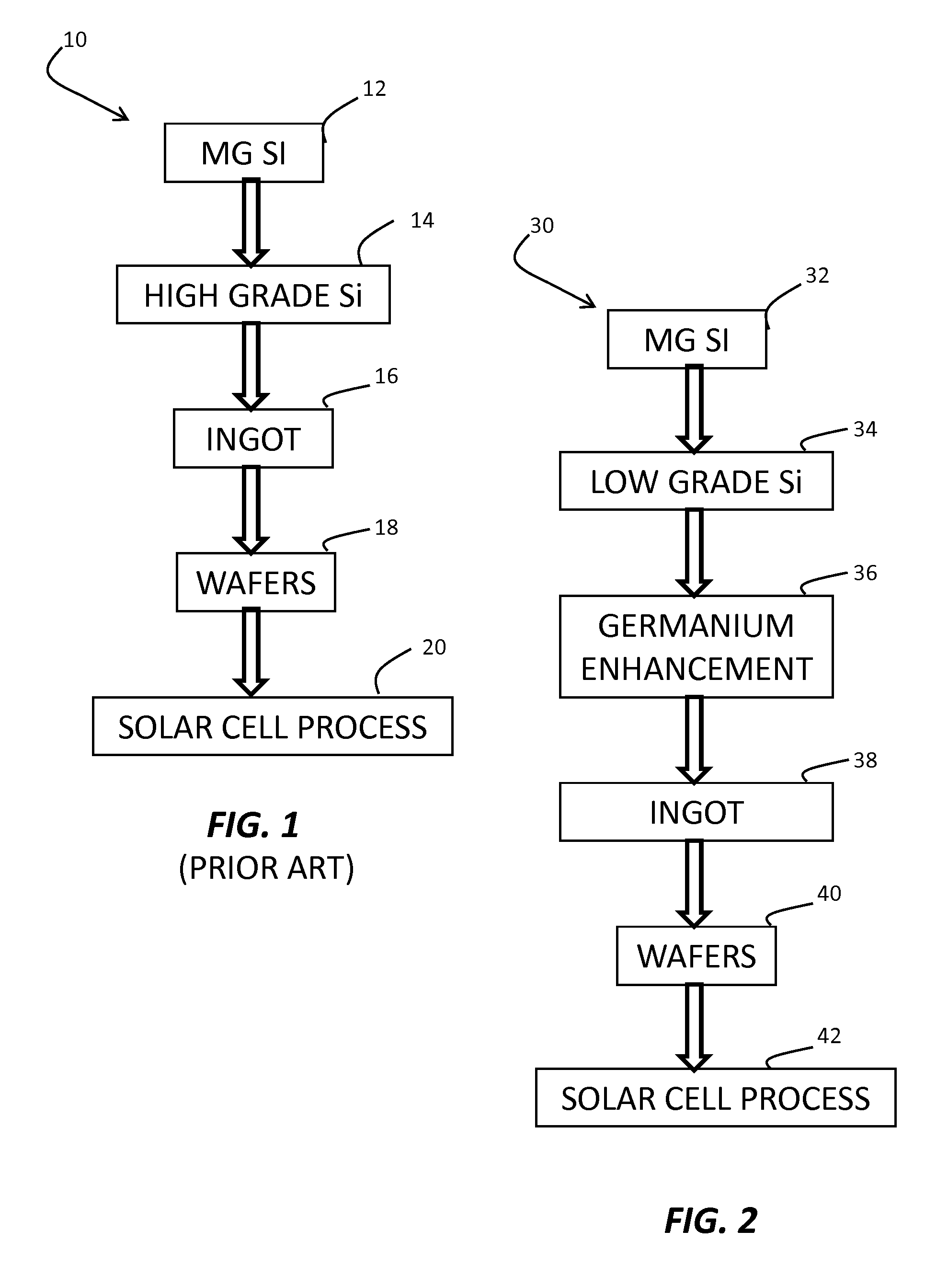
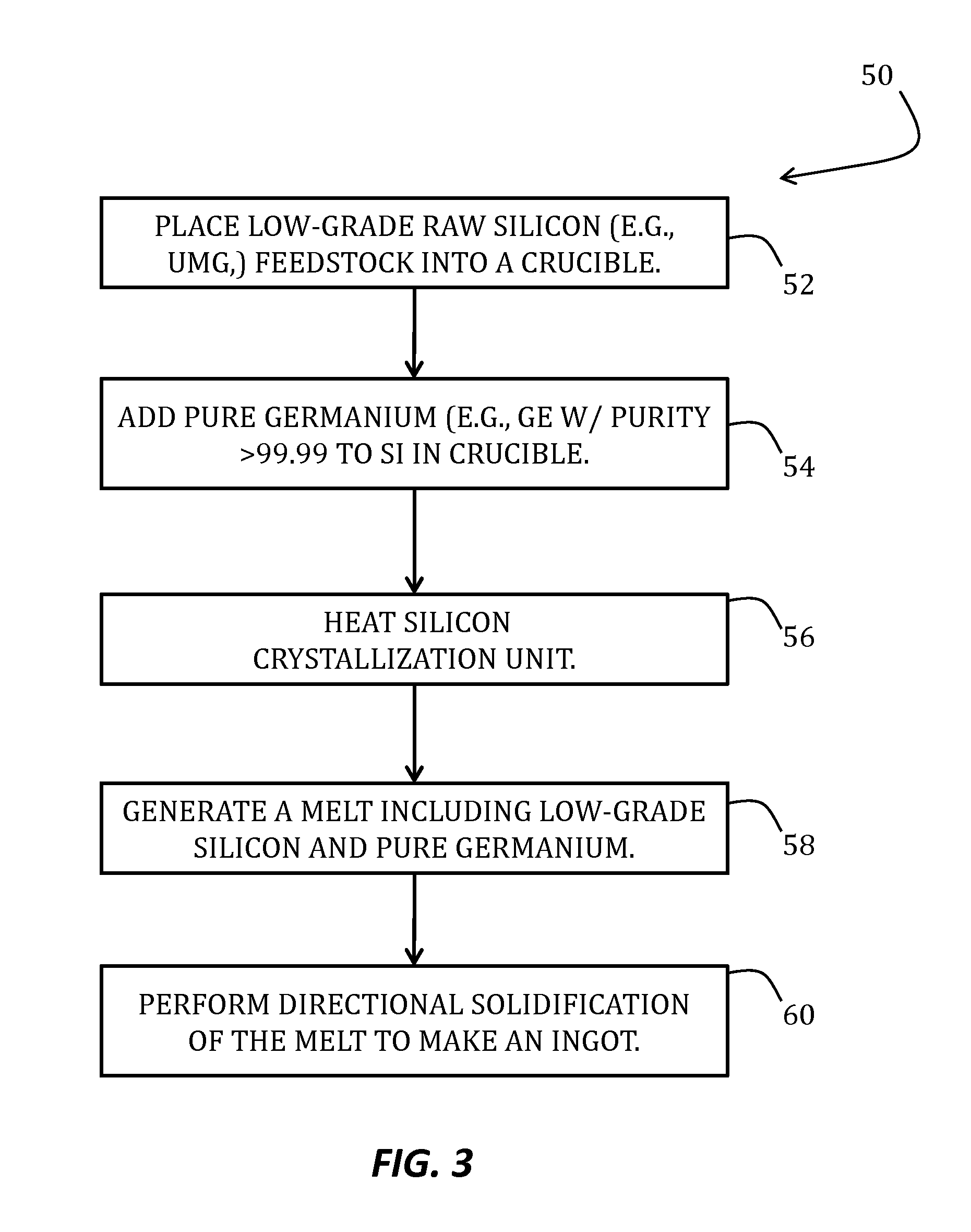
[0024]The method and system of the present disclosure provide a semiconductor ingot formation process for producing a silicon ingot or crystal using a low purity or high purity silicon feedstock. As a result of using the presently disclosed subject matter, an improvement in the properties of ingots formed from low-grade semiconductor materials, such as upgraded metallurgical grade silicon (UMG) occurs. Such improvement allows use of UMG silicon, for example, in producing solar cells for applications in solar power generation. The method and system of the present disclosure, moreover, particularly benefits the formation of silicon-based solar cells using UMG or other non-electronic grade feedstock materials. The present disclosure may, therefore, allow the manufacture of solar cells in greater quantities and in a greater number of fabrication facilities than has heretofore been possible.

[0025]Laying a context for the present disclosure, FIG. 1 depicts a known process 10 beginning at ...


PUM

PropertyMeasurementUnit
mechanicalaaaaaaaaaa
electrical characteristicsaaaaaaaaaa
purityaaaaaaaaaa

Abstract

Techniques for the formation of silicon ingots and crystals using silicon feedstock of various grades are described. Common feature is adding a predetermined amount of germanium to the melt and performing a crystallization to incorporate germanium into the silicon lattice of respective crystalline silicon materials. Such incorporated germanium results in improvements of respective silicon material characteristics, mainly increased material strength. This leads to positive effects at applying such materials in solar cell manufacturing and at making modules from those solar cells. A silicon material with a germanium concentration in the range (50-200) ppmw demonstrates an increased material strength, where best practical ranges depend on the material quality generated.

Description

FIELD[0001]The present disclosure relates to methods and systems for use in the fabrication of semiconductor materials such as silicon, for example using lower-grade silicon. More particularly, the present disclosure relates to a method and system for forming a silicon crystal or ingot with improved characteristics, including greater strength and flexibility, using feedstock material of various grades and germanium enrichment.DESCRIPTION OF THE RELATED ART[0002]The photovoltaic (PV) industry is growing rapidly and is responsible for an increasing amount of silicon being consumed beyond the more traditional uses as integrated circuit (IC) applications. Today, the silicon needs of the solar cell industry are partially competing with the silicon needs of the IC industry. With present manufacturing technologies, both IC and PV industries require a refined, purified, silicon feedstock as a raw silicon starting material.[0003]Materials alternatives for the bulk of current solar cells rang...

Claims


Application Information

Patent Timeline
Patent Type & Authority Applications(United States)
IPC IPC(8): H01L31/00C30B15/00C30B15/14
CPCC30B11/00Y10T117/1024C30B11/08C30B13/00C30B13/08C30B13/10C30B15/00C30B15/02C30B15/04C30B29/06H01L31/028C30B11/04Y10T117/1068Y02E10/547C30B29/52H01L31/00H01L31/18
Inventor KIRSCHT, FRITZABROSIMOVA, VERAHEUER, MATTHIASJOUINI, ANISLINKE, DIETERKAES, MARTINRAKOTONIAINA, JEAN PATRICEOUNADJELA, KAMEL
Owner HIGHLAND MATERIALS INC
Why Eureka
Try Eureka