Opto-Electrical Devices and Methods of Manufacturing the Same

a technology of opto-electrical devices and organic materials, applied in the direction of non-metal conductors, conductors, thermoelectric devices, etc., can solve the problems of lateral conduction, too high conductivity, and many significant problems, and achieve the effect of less polarity, improved film uniformity, and greater wetting capacity

Active Publication Date: 2009-12-24
CAMBRIDGE DISPLAY TECH LTD
View PDF20 Cites 10 Cited by
  • Summary
  • Abstract
  • Description
  • Claims
  • Application Information

AI Technical Summary

Benefits of technology

[0030]It has surprisingly been found that the provision of an alcohol ether additive having a boiling point lower than 170° C. results in a composition that has much better ink-jet directionality. That is, the spreading angle of droplets of the composition deposited by ink-jet printing is reduced by the presence of the additive. This is hugely beneficial for ink-jet printing of, for example, organic light-emissive displays, particularly when the pixel size of such displays is very small. The present invention reduces the possibility of ink being deposited in the wrong ink-well, or on a side of an ink-well rather than in the centre. While not being bound by theory, it is believed that the improvement in ink-jet directionality is due to a change in the contact angle of the composition with the inkjet print head.
[0071]For example, in one embodiment, a PEDOT:PSS composition of 1:20 gives a poor swathe join, a composition of 1:30 gives a good swathe join, and a composition of 1:40 completely eliminates the swathe join effect. An increase in PSS decreases the conductivity of the composition. Accordingly, the excess PSS (above 1:20) is acting as an insulating material / conductivity modifier. PSS also increases surface energy thus aiding wetting.

Problems solved by technology

However, there are several significant problems.
For example, if a plurality of electrodes are provided in a device but only one continuous layer of conductive polymer extending over all the electrodes, then too high a conductivity can lead to lateral conduction (known as “cross-talk”).
Furthermore, if the conductive polymer is not covered by the overlying layer(s) of organic material between the conductive polymer and the cathode then there is a risk of shorting between the conductive polymer and the cathode.
A problem associated with ink jet printing of materials for organic opto-electrical devices is that the printing process involves printing stripes (or swathes) of ink (corresponding to the ink jet head width) which results in an inbuilt asymmetry in the drying environment.
With more evaporation taking place on the unprinted side more solute is deposited on this side and the film profile becomes asymmetric, resulting in visible non-uniformities in the resultant display.
Another problem associated with ink jet printing of organic opto-electrical devices such as those discussed above is that in the resultant device, the organic hole injecting layer can extend beyond the overlying organic semi-conductive layer providing a shorting path between the cathode and the anode at an edge of the well.
This problem is exacerbated if the contact angle of the conductive organic composition with the bank material is too low.
This problem is further exacerbated if the conductivity of the organic hole injecting layer is too high.
However, providing a more complex bank structure is expensive and increases the complexity of the manufacturing method for the device.
In addition to the aforementioned problems of depositing prior art compositions using ink jet printing, it has also been found that some compositions comprising conductive and semi-conductive organic material are also difficult, or indeed impossible, to deposit by other methods such as spin-coating.

Method used


Image

  • Opto-Electrical Devices and Methods of Manufacturing the Same
  • Opto-Electrical Devices and Methods of Manufacturing the Same
  • Opto-Electrical Devices and Methods of Manufacturing the Same

Examples


Embodiment Construction

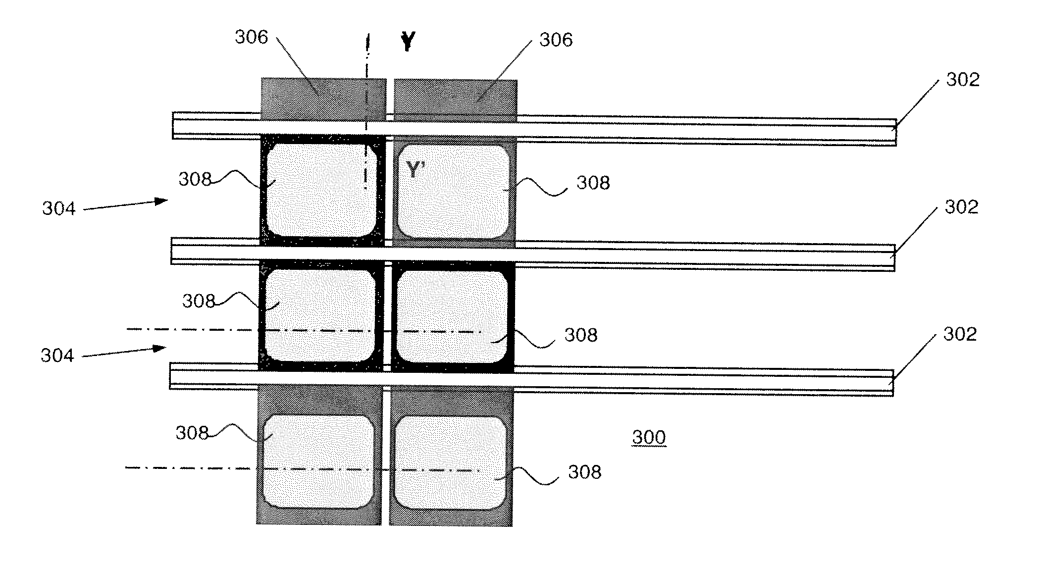
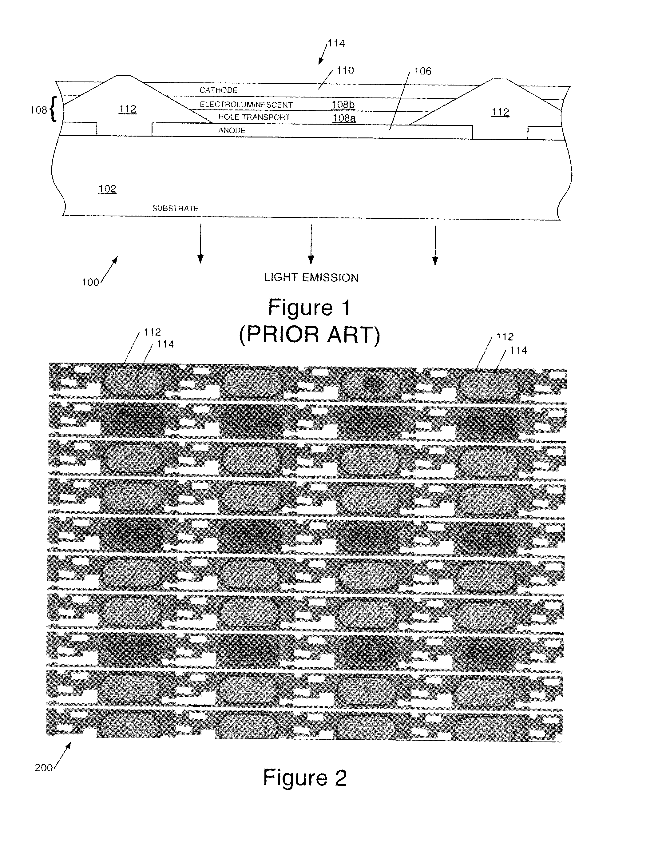
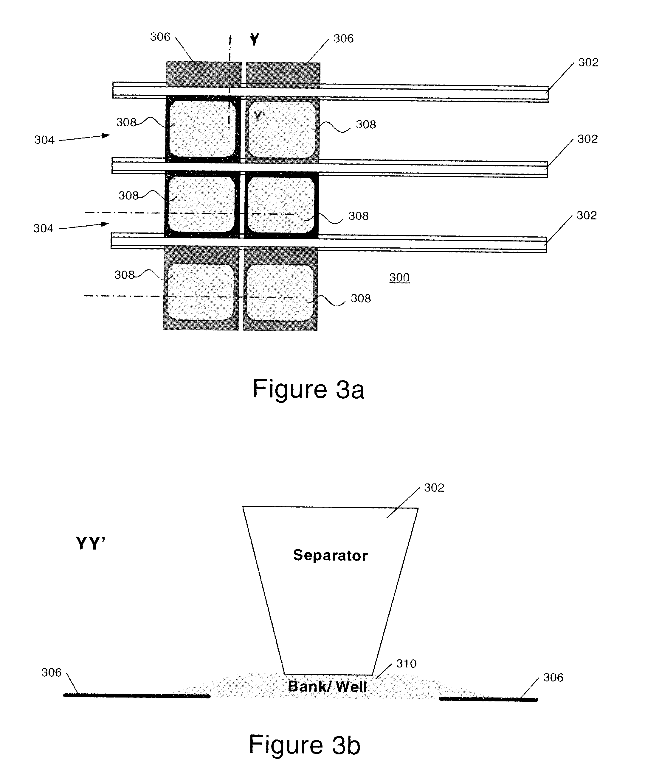
[0080]The general device architecture is illustrated in FIG. 1 and has been described above.

[0081]The device is preferably encapsulated with an encapsulant (not shown) to prevent ingress of moisture and oxygen. Suitable encapsulants include a sheet of glass, films having suitable barrier properties such as alternating stacks of polymer and dielectric as disclosed in, for example, WO 01 / 81649 or an airtight container as disclosed in, for example, WO 01 / 19142. A getter material for absorption of any atmospheric moisture and / or oxygen that may permeate through the substrate or encapsulant may be disposed between the substrate and the encapsulant.

[0082]Suitable polymers for charge transport and emission may comprise a first repeat unit selected from arylene repeat units, in particular: 1,4-phenylene repeat units as disclosed in J. Appl. Phys. 1996, 79, 934; fluorene repeat units as disclosed in EP 0842208; indenofluorene repeat units as disclosed in, for example, Macromolecules 2000, 33...


PUM

PropertyMeasurementUnit
boiling pointaaaaaaaaaa

Abstract

A composition for use in the manufacture of an opto-electrical device, the composition comprising: a conductive or semi-conductive organic material; a solvent; and a first additive, wherein the first additive is an alcohol ether having a boiling point lower than 170° C.

Description

FIELD OF INVENTION [0001]This invention relates to compositions for conductive or semi-conductive organic material, opto-electrical devices manufactured using these compositions, and methods of manufacturing these opto-electrical devices.BACKGROUND OF INVENTION [0002]One class of opto-electrical devices is that using an organic material for light emission (or detection in the case of photovoltaic cells and the like). The basic structure of these devices is a light emissive organic layer, for instance a film of a poly (p-phenylenevinylene) (“PPV”) or polyfluorene, sandwiched between a cathode for injecting negative charge carriers (electrons) and an anode for injecting positive charge carriers (holes) into the organic layer. The electrons and holes combine in the organic layer generating excitons which then undergoes radiative decay to give light (in light detecting devices this process essentially runs in reverse). In WO90 / 13148 the organic light-emissive material is a polymer. In U...

Claims


Application Information

Patent Timeline
Patent Type & Authority Applications(United States)
IPC IPC(8): H01L51/54H01B1/12B05D5/12H01L51/56
CPCH01L27/3246H01L27/3283H01L51/5088H01L51/0007H01L51/0037H01L51/0005H10K59/173H10K71/15H10K71/135H10K59/122H10K85/1135H10K50/17
Inventor WALLACE, PAULGODDARD, SIMON
Owner CAMBRIDGE DISPLAY TECH LTD
Why Eureka
Try Eureka