Organic light emitting display device and method for fabricating the same

a light-emitting display and organic technology, applied in the manufacture of electrode systems, electric discharge tubes/lamps, discharge tubes luminescnet screens, etc., can solve the problems of deterioration of numerical aperture (na), high power consumption, and difficulty in large-area display, so as to prevent short circuit, improve the lifespan, and improve the effect of morphology

Active Publication Date: 2009-12-24
LG DISPLAY CO LTD
View PDF4 Cites 19 Cited by
  • Summary
  • Abstract
  • Description
  • Claims
  • Application Information

AI Technical Summary

Benefits of technology

[0028]An advantage of the present invention is to provide an organic LED device capable of preventing a short circuit between an anode electrode and a cathode electrode using an organic passivation layer having favorable morphology, and improving the lifespan thereof by removing moisture inside the OLED device by forming a calcium (Ca) layer, and a method for fabricating the same.
[0029]Additional advantages, and features of the invention will be set forth in part in the description which follows and in part will become apparent to those having ordinary skill in the art upon examination of the following or may be learned from practice of the invention. The objectives and other advantages of the invention may be realized and attained by the structure particularly pointed out in the written description and claims hereof as well as the appended drawings.
[0030]To achieve these and other advantages and in accordance with the purpose of the invention, as embodied and broadly described herein, an OLED device comprises a substrate divided into pixel regions and non-pixel regions, thin film transistors (TFT) on the substrate, an organic passivation layer on an entire surface of the substrate including the TFTs, first electrodes on the organic passivation layer of the pixel regions to connect to the respective TFTs, organic emission layers on the respective first electrodes, a second electrode on an entire surface of the substrate including the organic emission layers, partitions on the organic passivation layer in the non-pixel regions to define the respective pixel regions, and first moisture absorbent layers between the respective partitions and the organic passivation layer.
[0031]The OLED device may further comprise a second moisture absorbent layer on the second electrode.
[0032]In another aspect of the present invention, a method for fabricating an OLED device comprises; preparing a substrate divided into pixel regions and non-pixel regions; forming thin film transistors on the substrate; forming an organic passivation layer on an entire surface of the substrate including the thin film transistors; forming contact holes in the organic passivation layer to expose drain electrodes of the thin film transistors; forming first electrodes on the organic passivation layer of the pixel regions to contact to the drain electrodes through the contact holes; forming first moisture absorbent layers on the organic passivation layer of the non-pixel regions; forming partitions in the non-pixel regions to cover the first moisture absorbent layers; forming organic emission layers on the first electrodes; and forming a second electrode on the an entire surface of the substrate including the organic emission layers.

Problems solved by technology

However, much power is consumed, and it is difficult to implement a large-area display.
In addition, the numerical aperture (NA) is deteriorated as the number of lines increases.
Such organic layers are subject to decomposition due to moisture from the outside and moisture outgassed from the inside.
Therefore, it is difficult to guarantee a sufficient lifespan of the device as a display device.

Method used


Image

  • Organic light emitting display device and method for fabricating the same
  • Organic light emitting display device and method for fabricating the same
  • Organic light emitting display device and method for fabricating the same

Examples


Embodiment Construction

[0041]Reference will now be made in detail to embodiments of the present invention, examples of which are illustrated in the accompanying drawings. Wherever possible, the same reference numbers will be used throughout the drawings to refer to the same or like parts.

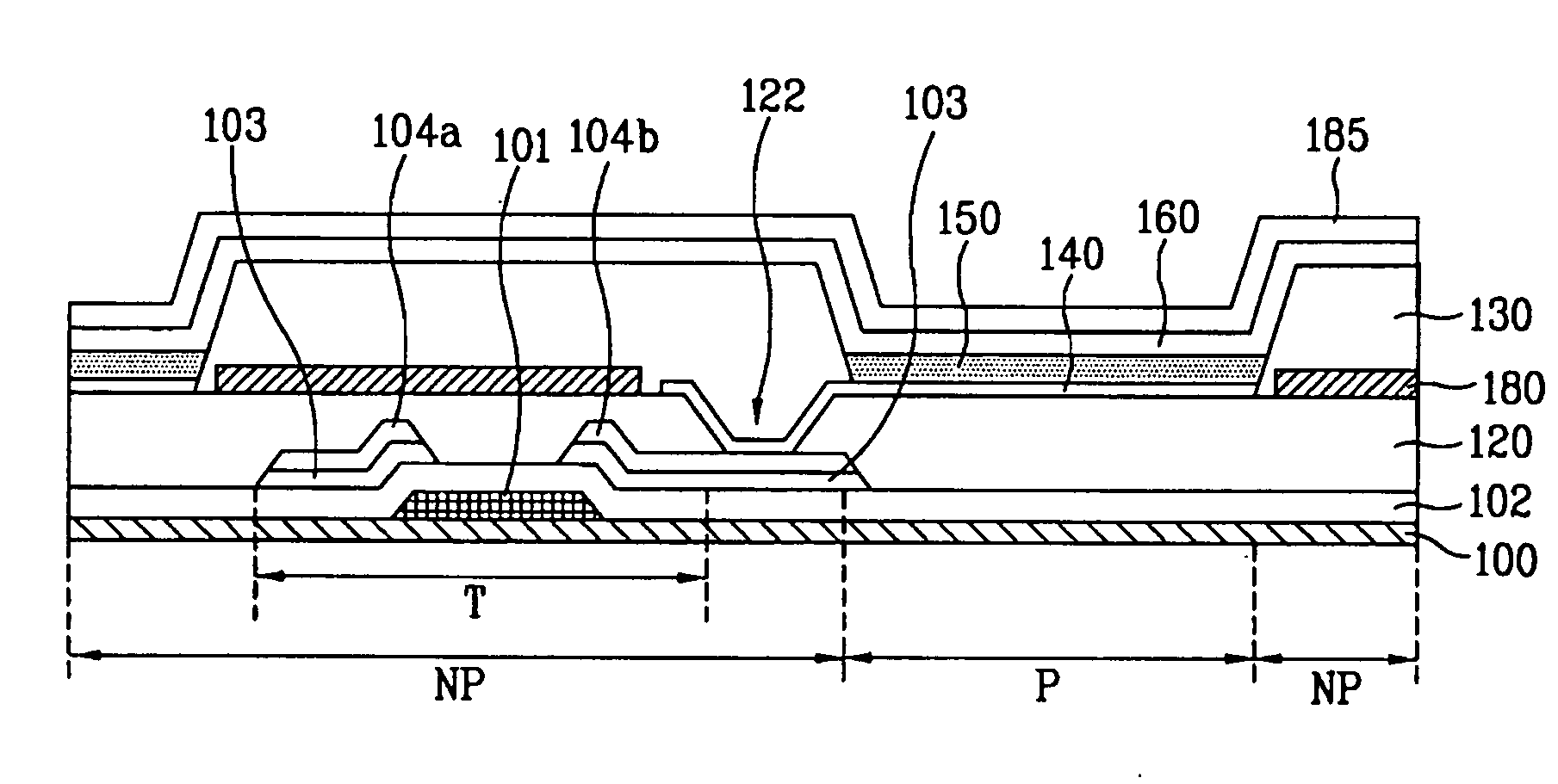
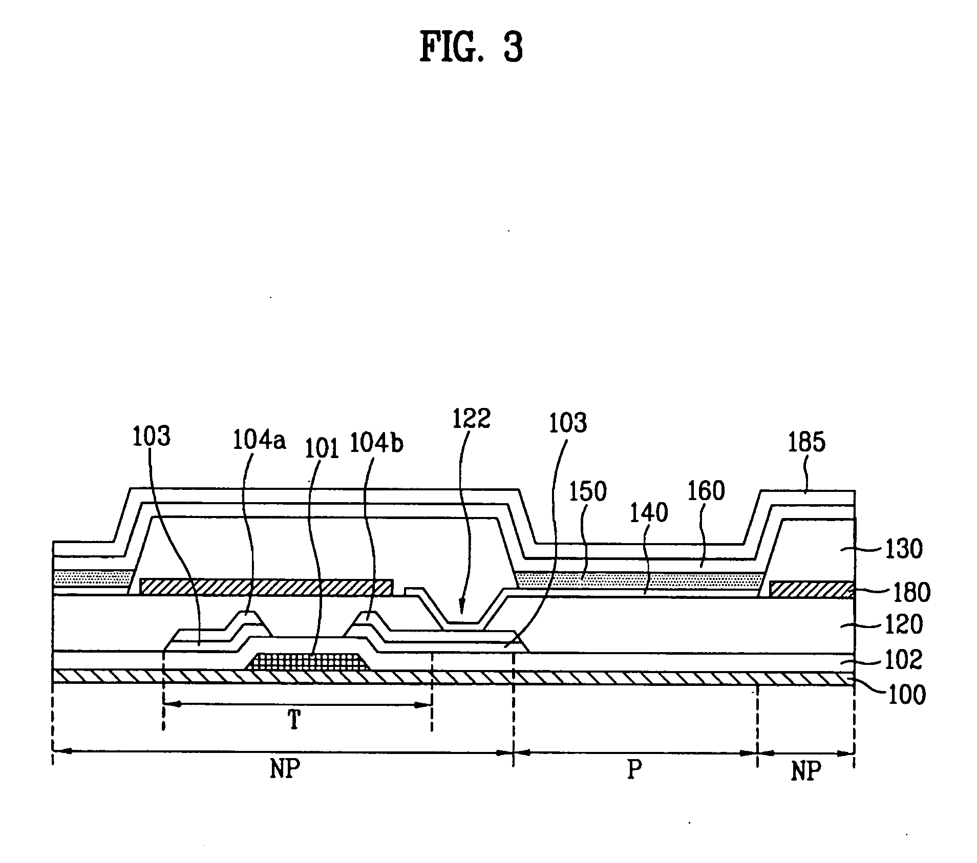
[0042]FIG. 3 is a sectional view of an organic light emitting display (OLED) device according to an embodiment of the present invention.

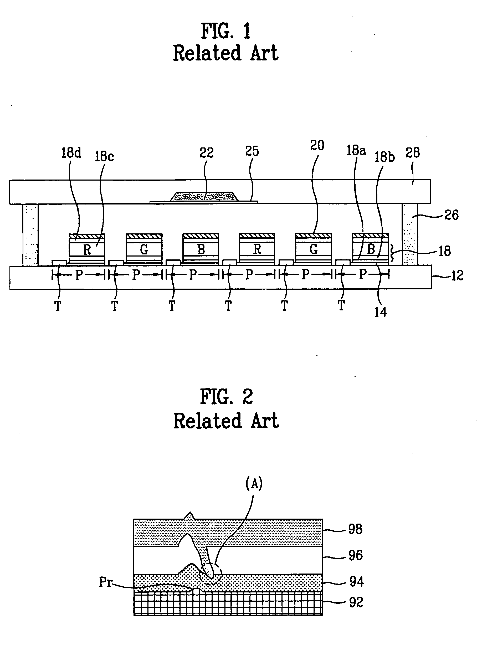
[0043]Referring to FIG. 3, the OLED device according to this embodiment comprises a substrate 100 in which a plurality of pixel regions P are arranged in a matrix form and non-pixel regions NP are arranged in the part excluding the pixel regions are defined, partitions 130 formed in the non-pixel regions NP to define the respective pixel regions P, thin film transistors (TFT) T formed on the substrate 100 to drive pixels, an organic passivation layer 120 of an organic material covering the whole surface of the substrate 100 including the TFTs T, first electrodes 140 connected to the TFTs ...


PUM


Abstract

An OLED device and a method for fabricating the same are disclosed, capable of improving yield and preventing decomposition of organic layers by moisture. An organic passivation layer having excellent morphology is applied to prevent a short circuit between an anode electrode and a cathode electrode. A Ca layer is applied to remove moisture from the inside of the device, thereby increasing the lifespan of the device. Accordingly, generation of dark sports by the short circuit caused by protrusions on a poor-morphology layer can be prevented. In addition, moisture absorbent layers are formed between the passivation layers and the partitions to remove outside moisture and the moisture outgassed from the inside, that is, partitions and organic layers, thereby elongating the lifespan of the OLED device.

Description

[0001]This application claims the benefit of Korean Patent Application No. 10-2008-059894, filed on Jun. 24, 2008, which is hereby incorporated by reference for all purposes as if fully set forth herein.BACKGROUND OF THE INVENTION[0002]1. Field of the Invention[0003]The present invention relates to an organic light emitting display (LED) device and a method for fabricating the same, and more particularly, to an organic LED device structured to prevent decomposition of organic layers caused by moisture, and a method for fabricating the same.[0004]2. Discussion of the Related Art[0005]With developments in the information-oriented society, demands for a new type of image displaying device to overcome shortcomings of the related art cathode ray tubes (CRT), such as its great weight and volume, have been increasing. In order to meet such demands, a variety of flat panel displays have been developed and spotlighted, including a liquid crystal display (LCD), an organic light emitting diode...

Claims


Application Information

Patent Timeline
Patent Type & Authority Applications(United States)
IPC IPC(8): H01J1/62H01J9/00
CPCH01L27/3246H01L51/5259H01L27/3258H10K59/122H10K59/124H10K50/846H01L2924/13069H10K10/88
Inventor KIM, DONG HWANYANG, MI YOUNKIM, HYUNG CHULLEE, JUN HOOH, KYUNG TAK
Owner LG DISPLAY CO LTD
Why Eureka
Try Eureka