
Eureka
For R&D, Eureka makes reading and utilizing patents & technical documents easy.
Eureka AIR
Designed for self-driven R&D workflows. Generate viable solutions, solve complex R&D challenges, empower your innovation with AI.

Eureka Materials
Designed for material experts only. Revolutionize your material R&D, from search, analyze, to developing new materials.

TechResearch
Generate reliable direction feasibility study reports for your R&D in just a few steps.

TechSeek
Discover and master advanced knowledge NOW. Basics, ideas, possibilities, all at once.

TechMind
As an expert in R&D Theories, TechMind can generates customized viable solutions instantly.

TechRisk
Analyze your overall solution with one click, know your potential R&D risks in advance.

TechMonitor
Get weekly tech updates, stay abreast of the latest tech innovations and key insights.
In-cell current subtraction for infrared detectors
- Summary
- Abstract
- Description
- Claims
- Application Information
AI Technical Summary
Benefits of technology
Problems solved by technology
Method used
Image

Examples
embodiment 200
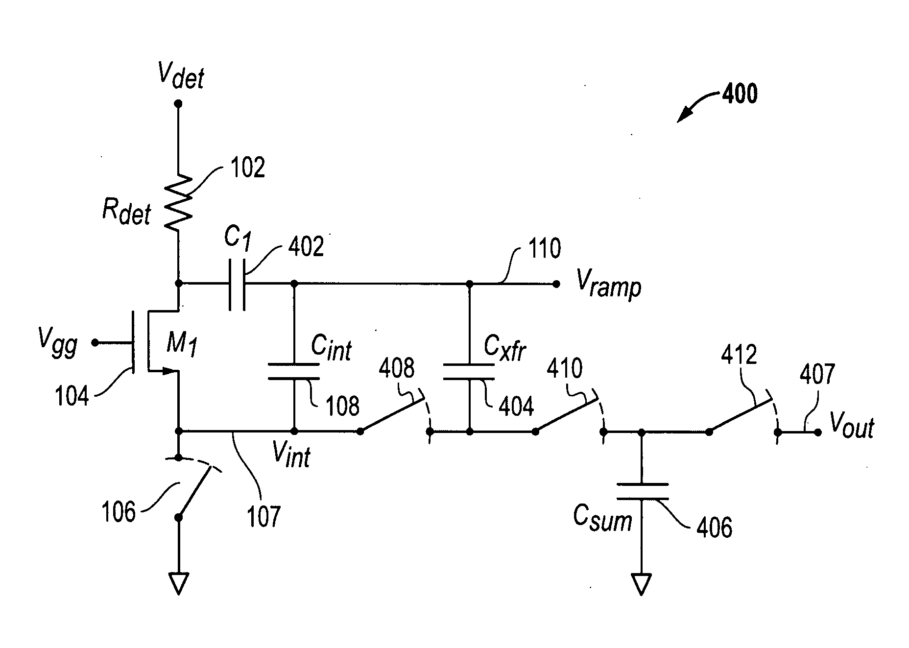
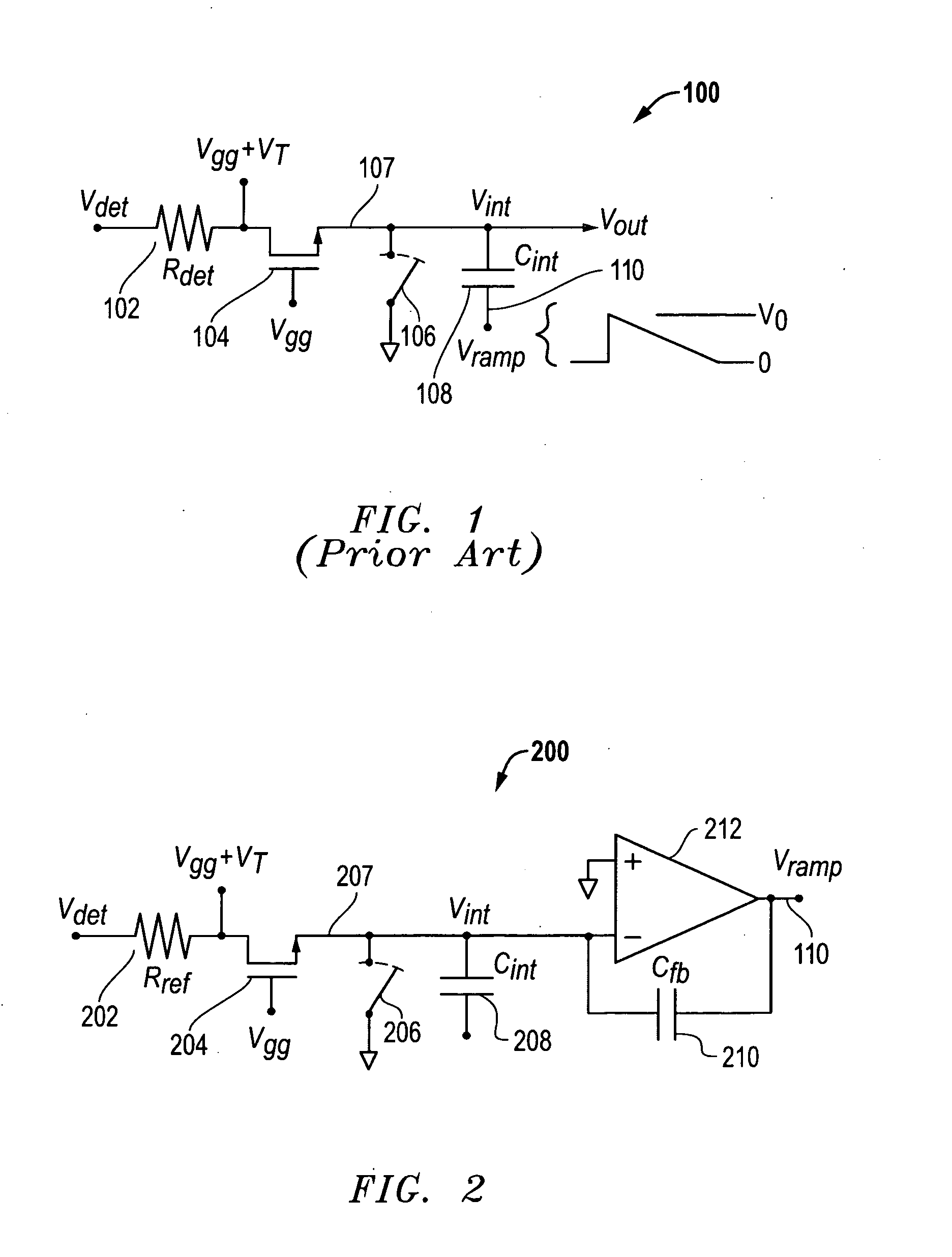
[0021]A feedback capacitor (Cfb) 204 is coupled between the Vramp node 110 and the negative (“−”) input to the amplifier 212. The feedback capacitor (Cfb) 204 may be used in place of the integration capacitor (Cint) 208, if desired, or it may supplement it, as shown in FIG. 2. If the feedback capacitor (Cfb) 204 is used in place of the integration capacitor (Cint) 208, then the integration capacitor (Cint) 208 is simply removed in embodiment 200 leaving only the feedback capacitor (Cfb) 204. In addition, there may be more than one resistor and transistor combination feeding current to the Vint node 107. Alternatively, there may be more than one resistor and a single transistor sized to accommodate the current from all the resistors. As depicted, transistor 104 and reference resistor (Rref) 202 are being used to feed current to the Vint node 207. Further, it is noted that the number of reference resistors and the value of the effective integration capacitance should be balanced to pr...
embodiment 300
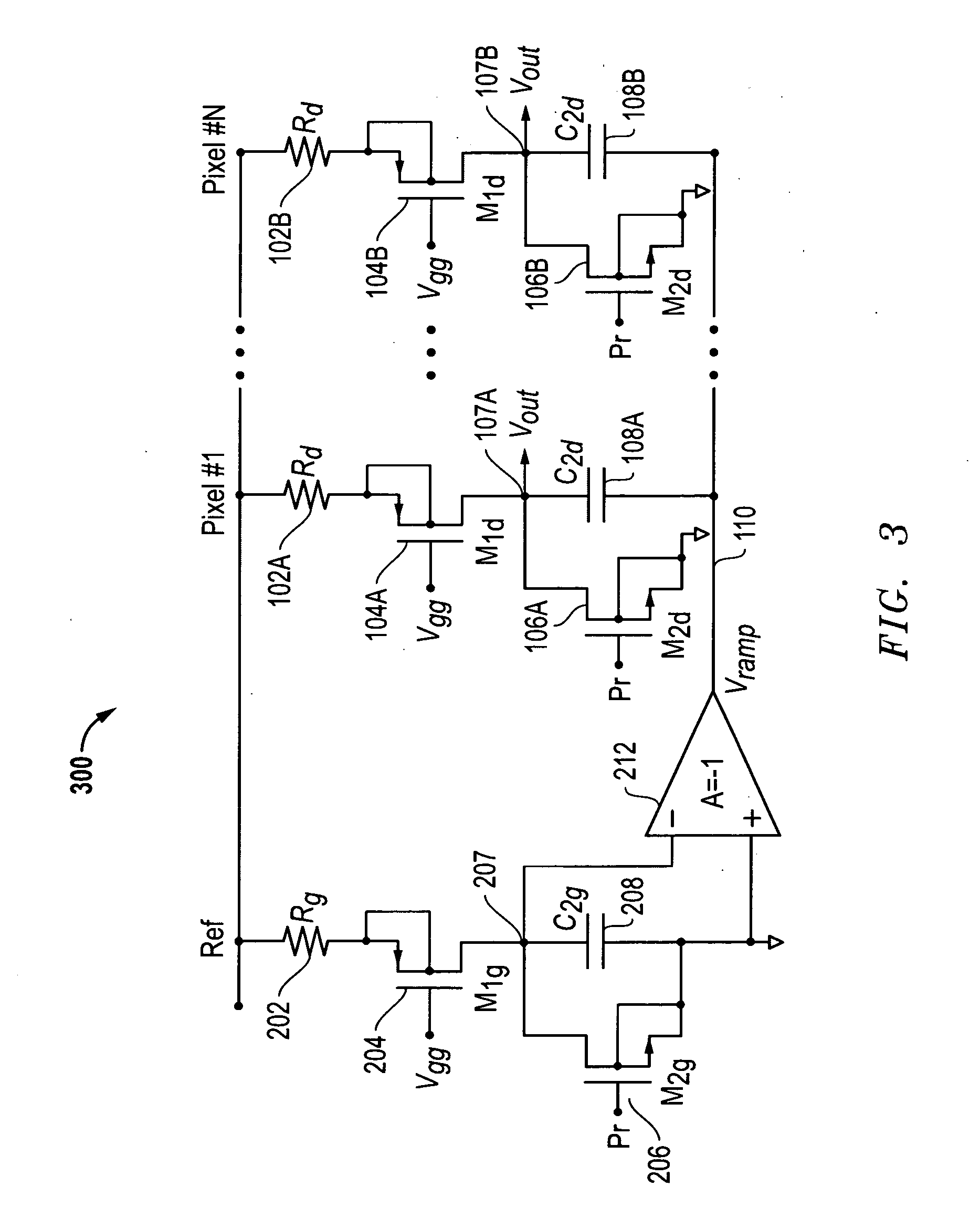
[0022]FIG. 3 is a circuit diagram of an embodiment 300 showing a ramp generator operating with a plurality of imaging pixels. The resistor Rg 202 represents a reference bolometer resistance that is not exposed to radiant energy from the scene, but rather is exposed to a source near ambient temperature. Alternatively, as indicated above, the resistor Rg 202 can be exposed to a blurred image of the scene in order for the incident energy to be an average scene radiance. As depicted, the voltage ramp (Vramp) output 110 is provided to a plurality of N pixels including Pixel #1 . . . Pixel #N. It is noted that the Vdet line at the top of FIG. 3 represents a bias voltage provided to the reference pixel / resistor Rg 202 and the plurality of detector pixels / resistors (Rd) 102A . . . 102B for the plurality of N pixels.
[0023]It is noted that for the plurality of pixel detectors Pixel #1 . . . Pixel #N, the circuits of FIG. 1 (prior art) repeat. As such, these common elements are referred to wit...
embodiment 500
[0028]FIG. 5 is a circuit diagram of an embodiment 500 for an alternative ramp generation circuit. More particularly, this alternative embodiment includes the addition of a temperature-independent fixed current source 502 and another integrating capacitor (Cfixed) at the positive (“+”) input of the amplifier 212 in the ramp generator of FIG. 2. The amplitude of the ramp created by reference pixels is adjusted (e.g., by adjusting the values of Cint 208, Cfb 210, and / or the amplitude of the temperature-dependent current source from transistor 204) so that the current subtracted without the temperature-independent fixed current source 502 is equal to the average current generated by the active pixels. Thus, the net average current after subtraction is approximately zero. The amplitude of the temperature-independent fixed current source 502 is then set by adjusting the amplitude of the fixed current source 502 and the value of the additional capacitor (Cfixed) so that the average net pi...
PUM
 Abstract
Description
Claims
Application Information
 - R&D Engineer
- R&D Manager
- IP Professional
- Industry Leading Data Capabilities
- Powerful AI technology
- Patent DNA Extraction
Browse by: Latest US Patents, China's latest patents, Technical Efficacy Thesaurus, Application Domain, Technology Topic, Popular Technical Reports.
© 2024 PatSnap. All rights reserved.Legal|Privacy policy|Modern Slavery Act Transparency Statement|Sitemap|About US| Contact US: help@patsnap.com