

Wafer support device and component used for the same
a technology of support device and support ring, which is applied in the manufacture of basic electric elements, semiconductor/solid-state devices, electric devices, etc., can solve the problems of accelerate the erosion achieve the effect of cooling down the protection ring, preventing the lift-up and damage of the protection ring, and facilitating the production of the wafer support devi
- Summary
- Abstract
- Description
- Claims
- Application Information
AI Technical Summary
Benefits of technology
Problems solved by technology
Method used
Image

Examples
first embodiment
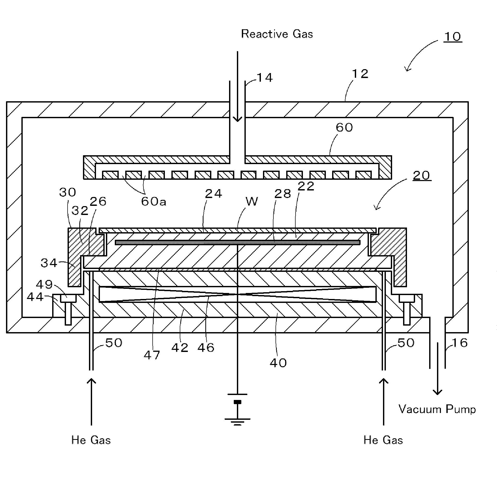
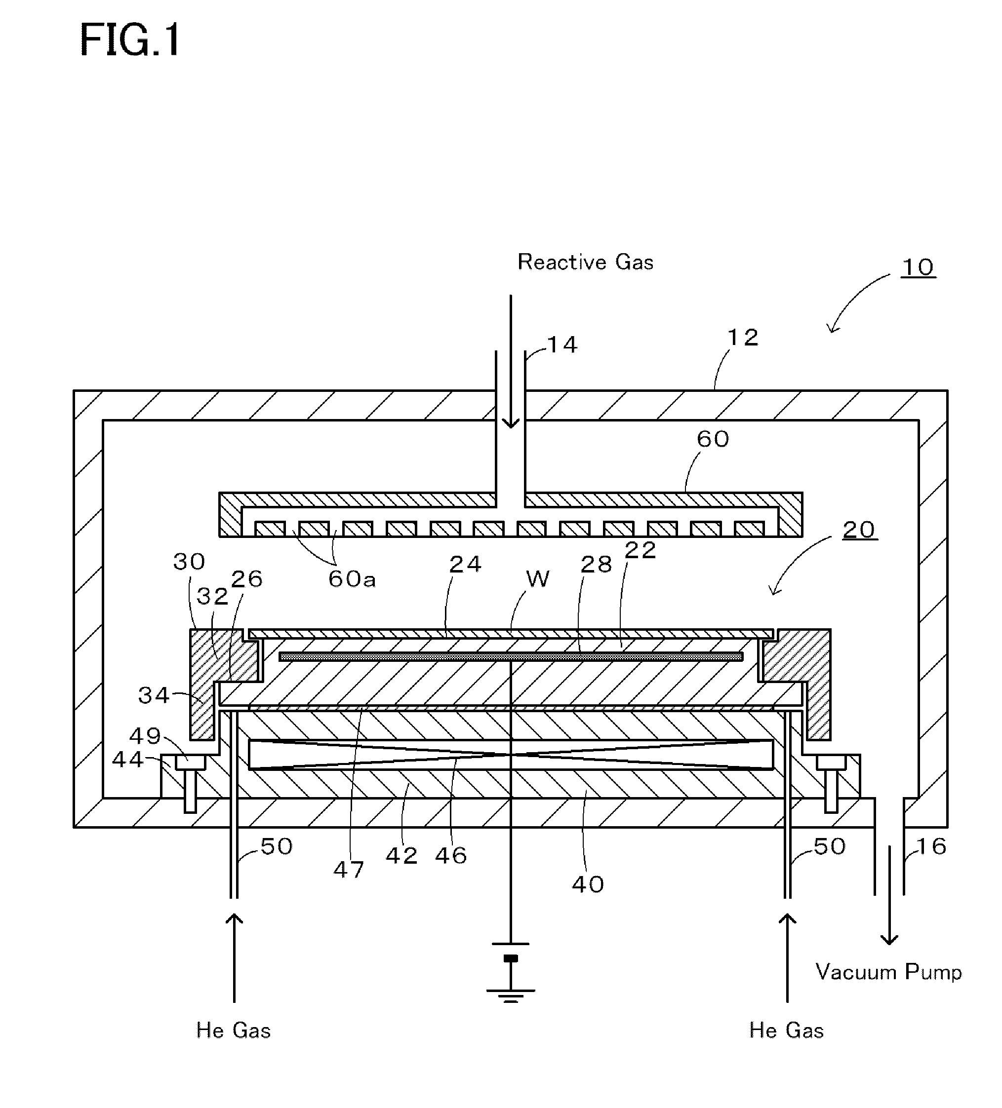
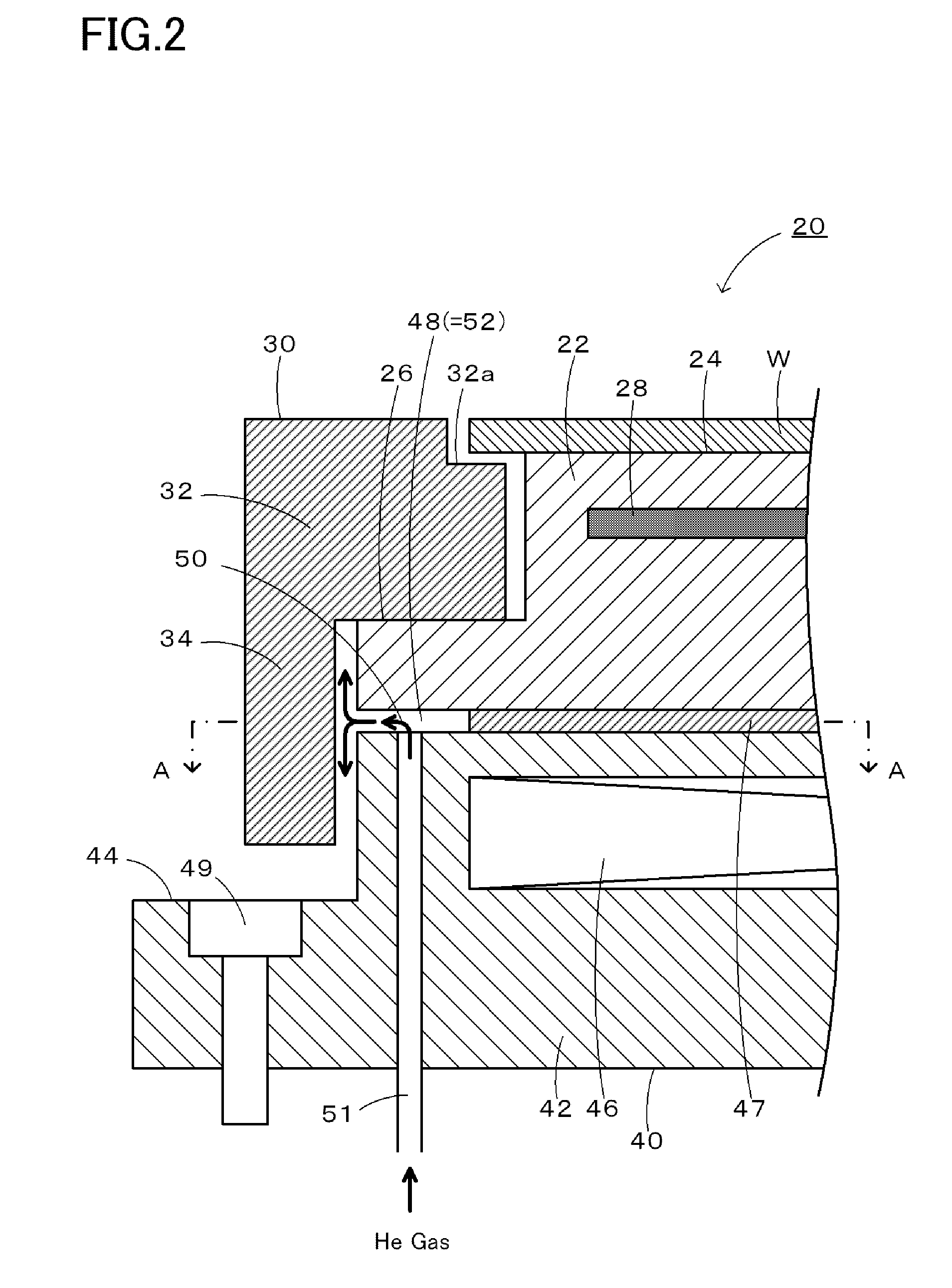
[0027]Some modes of carrying out the invention are described below as preferred embodiments with reference to the accompanied drawings. FIG. 1 is a sectional view schematically showing the configuration of a plasma processing apparatus 10 including a wafer support device 20 in a first embodiment of the invention. FIG. 2 is a partial sectional view of the wafer support device 20. FIG. 3 is a sectional view of the wafer support device 20, taken on the line A-A in FIG. 2.
[0028]In the plasma processing apparatus 10, the wafer support device 20 and an upper electrode 60 used for plasma generation are placed in a vacuum chamber 12 with the internal pressure adjustable function that is made of a metal (for example, an aluminum alloy) as shown in FIG. 1. The upper electrode 60 has a large number of small holes 60a for supplying a reactive gas to each wafer surface.
[0029]The vacuum chamber 12 is designed to introduce the reactive gas from a reactive gas supply conduit 14 onto the upper elect...
second embodiment
[0039]A wafer support device 120 is described below as a second embodiment of the invention. The wafer support device 120 of the second embodiment has structure similar to the structure of the wafer support device 20 of the first embodiment discussed above, except formation of a coolant gas flow path 150. The like components and elements of the second embodiment to those of the first embodiment are expressed by the like numerals and are not specifically described here. FIG. 4 is a partial sectional view of the wafer support device 120. FIG. 5 is a sectional view of the wafer support device 120, taken on the line B-B in FIG. 4.
[0040]In the wafer support device 120 of the second embodiment, the coolant gas flow path 150 is arranged to make a flow of helium gas as the coolant gas for cooling down the protection ring 30 as shown by the solid arrows in FIGS. 4 and 5. The coolant gas flow path 150 includes first flow paths 151 that are formed to pass through the horizontal refrigerant con...
working example 1
[0047]A wafer support device of Working Example 1 having the structure corresponding to the wafer support device 20 of the first embodiment was manufactured according to the procedure discussed below. The electrostatic chuck 22 was provided first. The procedure uniaxially molded aluminum nitride powder to an object of 5 mm in thickness and 380 mm in diameter, placed the molybdenum meshed internal electrode 28 (292 mm in diameter) on the molded object, added aluminum nitride powder on the internal electrode 28 in a mold, and formed a molded component of 25 mm as the whole thickness. The molded component was set with a graphite jig in a uniaxial hot press firing furnace and was fired under pressure of 1 ton in a nitrogen atmosphere at 1850° C. for 2 hours to obtain a sintered body with the internal electrode 28 embedded therein. The sintered body was subjected to cutting work to give the electrostatic chuck 22 having the following dimensions. The thickness from the internal electrode ...
PUM
 Abstract
Description
Claims
Application Information