

Plasma processing apparatus, plasma processing method and storage medium
a plasma processing and plasma technology, applied in the direction of plasma technique, chemical vapor deposition coating, coating, etc., can solve the problems of reducing the degree of freedom of plasma processing, difficult control of rf power, and inability to perform selection with a good precision, so as to effectively suppress the damage of the substrate by plasma and easily control the temperature of the processing chamber.
- Summary
- Abstract
- Description
- Claims
- Application Information
AI Technical Summary
Benefits of technology
Problems solved by technology
Method used
Image

Examples
first embodiment
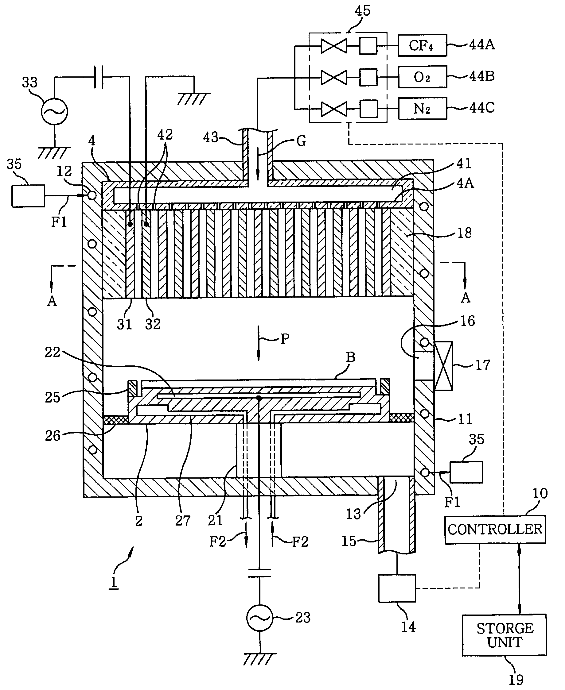
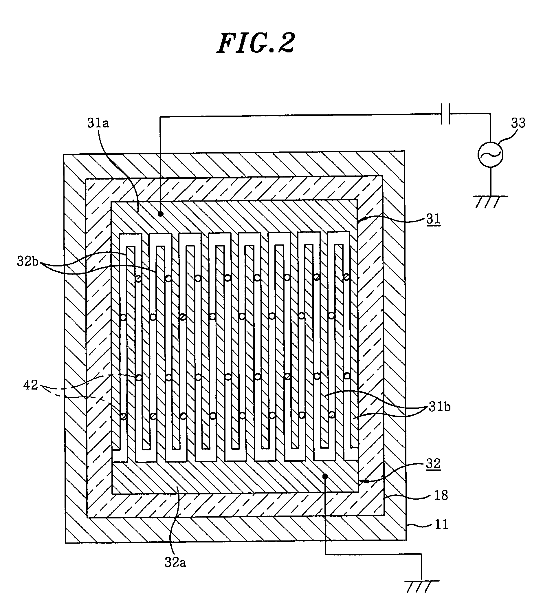
[0050]Referring to FIG. 1, a configuration of a plasma etching apparatus 1 in accordance with a first embodiment of the present invention will be described. The plasma etching apparatus 1 processes, e.g., a rectangular type substrate B such as an FPD (Flat Panel Display) or the like. The plasma etching apparatus 1 includes a tubular processing chamber 11 having enclosed sealed inner processing space, a mounting table 2 installed at a center region in a lower inner space of the processing chamber 11, electrodes 31, 32 provided above the mounting table 2 to generate plasma P, and a gas shower head (gas supply unit) 4 disposed above the electrodes 31, 32 to face the mounting table 2.
[0051]The processing chamber 11 is made of a metal, e.g., aluminum having a superior cooling ability than ceramic or the like, and inner surfaces of the processing chamber 11 are coated and insulated with, e.g., alumite. Further, the processing chamber 11 has flow channels 12 for a temperature adjustment fl...
second embodiment
[0071]Following is a description of a plasma etching apparatus 51 in accordance with another embodiment as shown in FIG. 5. The pair of the comb electrodes 31, 32 forming the first and second electrodes are provided under the gas shower head 4 in the above-mentioned embodiment, whereas one of the first and second electrodes is formed as a part of the gas shower head (gas supply unit) 52 and the other is formed as a comb electrode in this embodiment. Therefore, one comb electrode is provided under the gas shower head 52. In this etching apparatus 51, elements or units having the same configuration as them of the above-mentioned etching apparatus 1 use the same reference numerals as them of the etching apparatus 1.
[0072]The gas shower head 52 of the etching apparatus 51 is made of a metal such as aluminum or the like and the surface thereof is coated with an insulating material such as Y2O3 or the like. Moreover, the gas shower head 52 serves as the electrode connected to ground for g...
third embodiment
[0077]Following is a description of a plasma etching apparatus 56 in accordance with a still another embodiment as shown in FIG. 8. The plasma etching apparatus 56 includes a gas shower head 57 whose configuration will be explained with reference to FIG. 9.
[0078]The gas shower head 57 has a plate-type body 57D and is made of the same material as that of the gas shower head (gas supply unit) 52 of the second embodiment, e.g., aluminum. One of the first and second electrodes is formed as a part of the gas shower head (gas supply unit) 57 and the other is formed as a comb electrode 59 to be explained later. The gas shower head 57 is different from the gas shower head 52 in that a plurality of linear protrusions 58, which extend horizontally in parallel and spaced apart from each other, are arranged at a lower surface of the plate-type body 57D. Further, a plurality of gas supply holes 57b are formed in the lower surface of the plate-type body 57D between the linear protrusions 58 and i...
PUM
| Property | Measurement | Unit |
|---|---|---|
| Temperature | aaaaa | aaaaa |
| Diameter | aaaaa | aaaaa |
| Shape | aaaaa | aaaaa |
Abstract
Description
Claims
Application Information