Organic thin film solar cell

a solar cell and organic technology, applied in the field of organic thin film solar cells, can solve the problems of limited actual amount of work, low conversion efficiency, and extent to which charge-separated carriers are transported to the electrodes, and achieve the effect of improving the conversion efficiency of solar cells

Inactive Publication Date: 2010-01-21
PANASONIC CORP
View PDF9 Cites 21 Cited by
  • Summary
  • Abstract
  • Description
  • Claims
  • Application Information

AI Technical Summary

Benefits of technology

[0013]In the present invention, since the organic semiconductor molecules in which cyclic compounds are bound in a linear fashion lacks dispersibility with organic semiconductor molecules of fullerene and the like, the alternating stack thereof to form the multilayer film enables operation similar to that of the photoelectric conversion layer having a bulk heterojunction structure. In addition, carrier transportability can be improved due to the high mobility characteristics of the organic semiconductor molecules in which cyclic compounds are bound in a linear fashion.
[0018]It is required to enhance the conversion efficiency of the solar cell. So, it is preferred that the multilayer film further comprises an intermediate layer which is provided between the electron-donating organic semiconductor thin film and the electron-accepting thin film. The intermediate layer is preferably an electron donating organic semiconductor thin film having a band gap smaller than the adjacent electron-donating organic semiconductor thin film. Or, the intermediate layer is preferably an electron-accepting organic semiconductor thin film having a band gap smaller than the adjacent electron accepting thin film.

Problems solved by technology

However, in solar cells employing this configuration, since the diffusion length of the excitons is short at roughly only several tens of nanometers, carrier paths are actually able to be effectively formed only within a distance range of several tens of nanometers from the p-n junction interfaces, thus resulting in an extremely low conversion efficiency.
On the other hand, another important issue is the extent to which the charge-separated carriers are transported to the electrodes without being deactivated (recombined).
In other words, in the case there is imbalance in the numbers of electrons and holes collected, the actual amount of work is limited by that having the smaller number of carriers.
Although low molecular weight organic solar cells using fullerene for the n-type organic semiconductor are known to demonstrate high conversion efficiency, since the electron transport capacity of fullerene exceeds the hole transport capacity of p-type organic semiconductors, an excess of electrons end up being transported resulting in the hole transport capacity limiting the overall generated current.
Consequently, phthalocyanine ends up limiting the generated current resulting in the problem of decreased conversion efficiency.
However, since oligothiophene and pentacene are molecules in which cyclic compounds are bound in a linear fashion, they easily aggregate on the surface of a substrate during vapor deposition, thereby making it difficult to uniformly disperse molecules of the p-type organic semiconductor in molecules of the n-type organic semiconductor at the nanometer level, and resulting in the problem of it being difficult to effectively improve conversion efficiency.

Method used


Image

  • Organic thin film solar cell
  • Organic thin film solar cell
  • Organic thin film solar cell

Examples


example 1

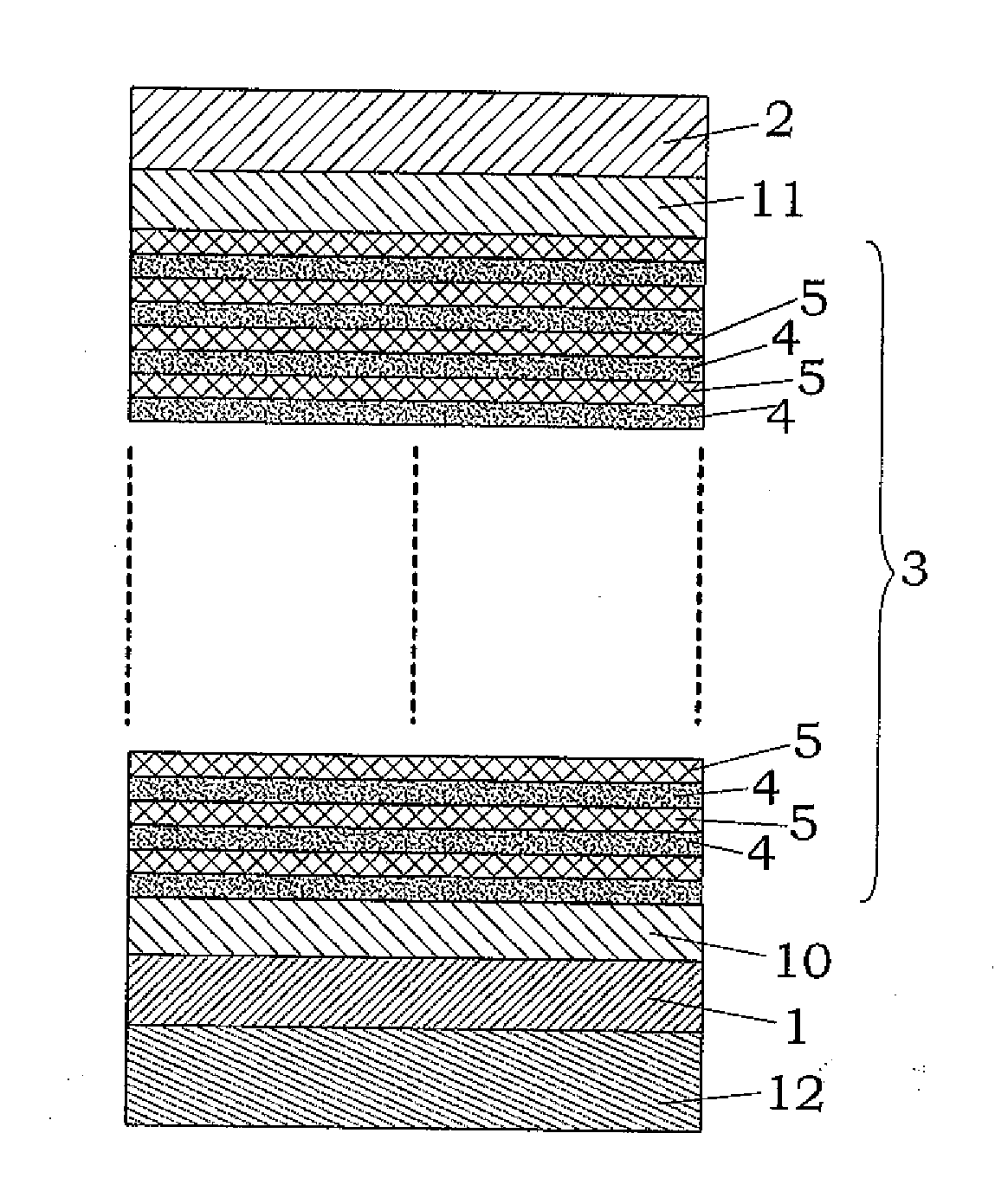
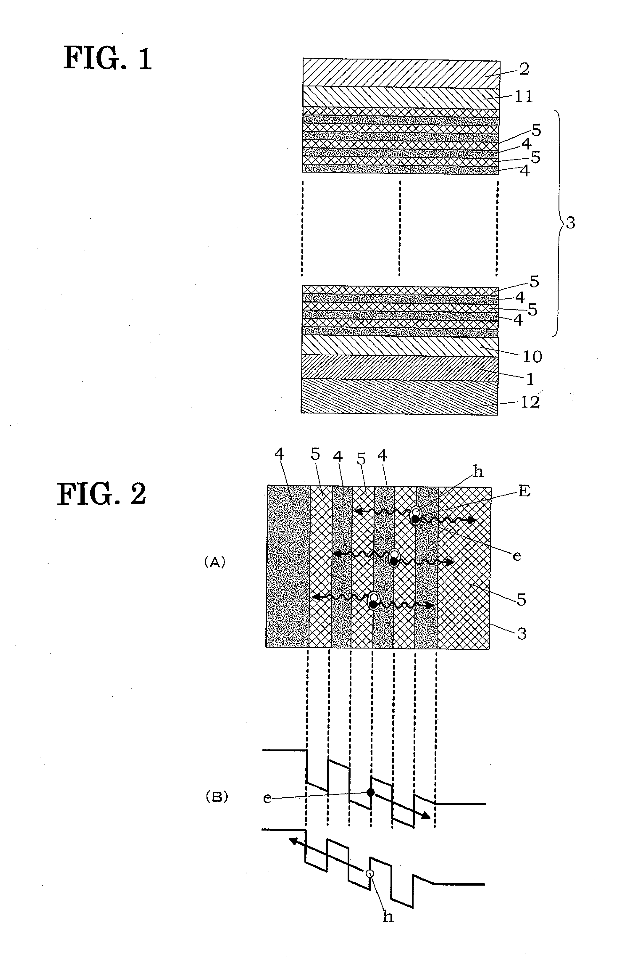
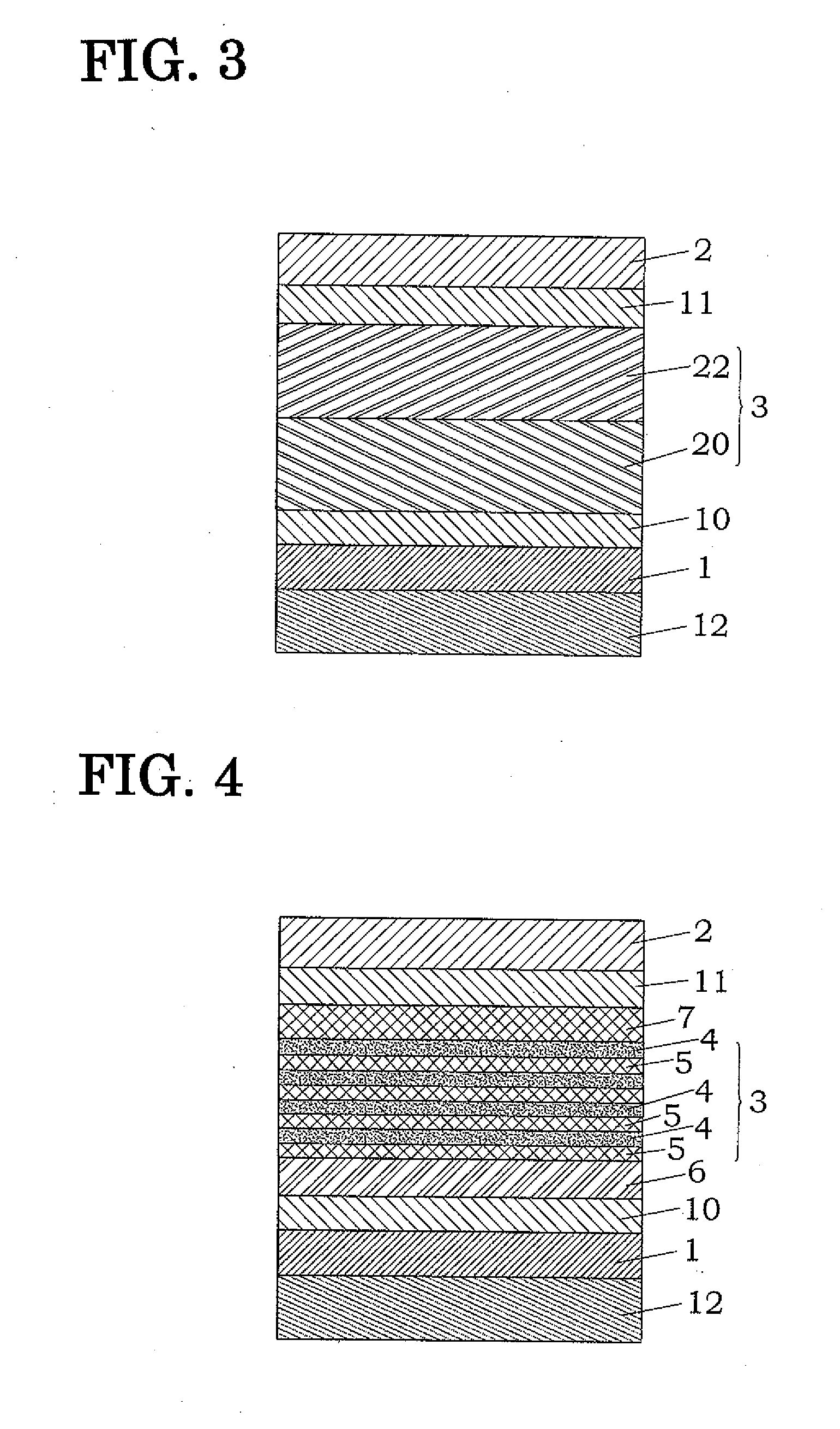
[0055]As shown in FIG. 4, a hole transport layer 10 in the form of a PEDOT:PSS layer (poly[3,4-(ethylenedioxy)thiophene]:poly (styrene sulfonate) was formed at a film thickness of 30 nm on an electrode 1 in the form of a glass electrode 12 in which an ITO electrode was formed a film thickness of 150 nm. Next, p-type organic semiconductor molecules in the form of pentacene were vacuum vapor-deposited on hole transport layer 10 to form an electron-donating organic semiconductor thin film 6 having a film thickness of 25 nm.

[0056]Next, n-type organic semiconductor molecules in the form of fullerene (C60) were vacuum vapor-deposited on thin film 6 to form electron-accepting organic semiconductor thin film 5 having a film thickness of 1 nm, and pentacene was vacuum vapor-deposited thereon to form electron-donating thin film 4 having a film thickness of 1 nm. The fullerene thin film 5 and pentacene thin film 4 were alternately stacked three times each to form a multilayer film in the form ...

example 2

[0058]An organic thin film solar panel of Example 2 was obtained in the same manner as Example 1 with the exception of photoelectric conversion layer 3 having a multilayer structure consisting of a total of four layers provided with two layers each of fullerene thin film 5 having a film thickness of 2 nm and pentacene thin film 4 having a film thickness of 2 nm, and in which these layers are alternately stacked.

example 3

[0059]An organic thin film solar panel of Example 3 was obtained in the same manner as Example 1 with the exception of photoelectric conversion layer 3 having a multilayer structure consisting of a total of six layers provided with three layers each of fullerene thin film 5 having a film thickness of 1 nm and pentacene thin film 4 having a film thickness of 2 nm, and in which these layers are alternately stacked.


PUM

PropertyMeasurementUnit
thicknessaaaaaaaaaa
optical transparencyaaaaaaaaaa
semiconductoraaaaaaaaaa

Abstract

The present invention provides an organic thin film solar cell having a novel photoelectric conversion layer with superior conversion efficiency from light to electricity and superior carrier transportability to an electrode. The photoelectric conversion layer is arranged between a pair of electrodes at least one of which has optical transparency, and comprises a multilayer film formed by alternately laminating an electron-donating organic semiconductor thin film and an electron-accepting thin film. The electron-donating organic semiconductor thin film is formed by organic semiconductor molecules in which cyclic compounds are bound in a linear fashion.

Description

TECHNICAL FIELD[0001]The present invention relates to an organic thin film solar cell that uses an organic semiconductor.BACKGROUND[0002]Organic thin film solar cells are expected to be used as future low-cost solar cells since they can be produced easier and with lower equipment costs than conventional silicon and compound semiconductor solar cells.[0003]In organic thin film solar cells of the p-n heterojunction type using p-type and n-type organic semiconductors, the organic semiconductors form excitons in which electron-hole pairs are strongly bound, and these diffuse and migrate to the interface of p-n junctions. Excitons are charge-separated into electrons and holes due the strong electric field at the interface, and the resulting electrons and holes are transported to respectively different electrodes resulting in the generation of electromotive force. However, in solar cells employing this configuration, since the diffusion length of the excitons is short at roughly only seve...

Claims


Application Information

Patent Timeline
Patent Type & Authority Applications(United States)
IPC IPC(8): H01L31/00
CPCB82Y10/00C08G2261/1424C08G2261/3223H01L51/0036H01L51/0046Y02E10/549H01L51/0078H01L51/4246H01L51/4253H01L2251/308H01L51/0055H10K85/113H10K85/211H10K85/623H10K85/311H10K30/211H10K30/30H10K2102/103H10K30/00
Inventor SAKAI, JUNSAITO, KAZUHIROSATIO, KUNIOSATIO, NAMIKOTAIMA, TETSUYA
Owner PANASONIC CORP
Why Eureka
Try Eureka