ESD protection device

a protection device and esd technology, applied in the direction of semiconductor/solid-state device details, soldering apparatus, manufacturing tools, etc., can solve the problems of reduced signal quality, poor heat resistance of formed organic-inorganic composite films, and tendency to change film characteristics, so as to improve productivity and cost effectiveness, reduce the effect of siz

Active Publication Date: 2010-01-28
TDK CORPARATION
View PDF9 Cites 10 Cited by
  • Summary
  • Abstract
  • Description
  • Claims
  • Application Information

AI Technical Summary

Benefits of technology

[0017]The thickness of the functional layer preferably ranges from 10 nm to 10 μm, more preferably from 10 nm to 1 μm. When the formed composite has a small thickness ranging from 10 nm to 10 μm as described above, an electronic apparatus using the ESD protection device can be further reduced in size while having high performance. Further, since a composite having an extremely thin thickness ranging from 10 nm to 1 μm can be formed by using a known method for forming a thin film, such as sputtering and deposition, the productivity and cost effectiveness can be enhanced. In other words, unlike an organic-inorganic composite film formed by conventional printing described above, a significant advantage consists in the fact that a composite of an insulating inorganic material and a conductive inorganic material to which a layer formation method, such as sputtering and deposition, can be applied is employed as the functional layer.
[0018]The insulating inorganic material is preferably at least one material selected from the group consisting of Al2O3, TiO2, SiO2, ZnO, In2O3, NiO, CoO, SnO2, V2O5, CuO, MgO, ZrO2, AlN, BN, and SiC. Any of these metal oxides, which excel in the insulating property, heat resistance, and weather resistance, effectively functions as a material that forms the insulating matrix of the composite, whereby a high-performance ESD protection device that excels in discharge characteristics, heat resistance, and weather resistance is achieved. Further, these metal oxides are available at low cost and sputtering can be applied to them, productivity and cost effectiveness can also be enhanced.
[0019]The conductive inorganic material is preferably at least one metal selected from the group consisting of C, Ni, Cu, Au, Ti, Cr, Ag, Pd, and Pt or any metal compound thereof Mixing any of the metals or metal compounds with the matrix of the insulating inorganic material in such a way that the metal or metal compound is discretely dispersed therein allows a high-performance ESD protection device that excels in discharge characteristics, heat resistance, and weather resistance to be achieved.
[0020]The functional layer is preferably a composite formed by successively or simultaneously sputtering the insulating inorganic material and the conductive inorganic material. In this way, a composite containing a conductive inorganic material discretely dispersed in a matrix of an insulating inorganic material can be obtained readily and reproducibly, whereby the productivity and cost effectiveness can be enhanced.
[0021]The present invention not only provides an ESD protection device that has small capacitance, excellent discharge characteristics, and enhanced heat resistance and weather resistance, but also allows the thickness of the ESD protection device to be further reduced as compared to the thickness having been achieved in related art and the productivity and cost effectiveness to be enhanced.

Problems solved by technology

An important technical challenge in this case is to protect electronic components from overvoltages represented by electrostatic pulses produced when the human body comes into contact with a terminal of an electronic apparatus.
However, large capacitance of a multilayer varistor, when used in a high-speed transmission system, causes reduction in signal quality.
A problem, therefore, is that the thus formed organic-inorganic composite film has poor heat resistance and the characteristics of the film tend to change with temperature, humidity, and other environmental conditions.
Further, since the metal particles or the metal oxide undergoes aggregation, segregation, or other phenomena during the preparation process of the organic-inorganic composite material and during the formation process of the organic-inorganic composite film, the overvoltage protection effect of the thus formed film tends to be non-uniform, resulting in poor reliability.
Further, in the antistatic components described in Patent Documents 1 to 3, since the organic-inorganic composite films are formed by using stencil printing, screen printing, or any other suitable method to apply the organic-inorganic composite film materials and drying the resultant structures or treating them in other processes, productivity and cost effectiveness are poor.
It is therefore difficult to further reduce the thickness of the organic-inorganic composite film without compromising the productivity and cost effectiveness.

Method used


Image

  • ESD protection device
  • ESD protection device
  • ESD protection device

Examples


first embodiment

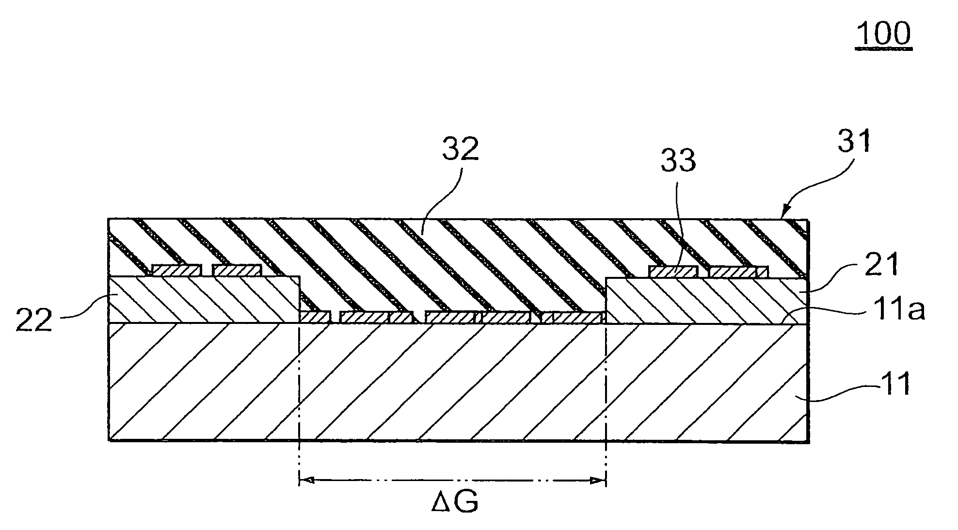
[0030]FIG. 1 is a diagrammatic cross-sectional view schematically showing a first embodiment of an ESD protection device according to the present invention. An ESD protection device 100 includes an insulating substrate 11, a pair of electrodes 21 and 22 disposed on the insulating substrate 11, a functional layer 31 disposed between the electrodes 21 and 22, and terminal electrodes 41 (see FIG. 6) electrically connected to the electrodes 21 and 22. The ESD protection device 100 is designed to allow the functional layer 31 to function as a low-voltage discharge-type electrostatic protection material and ensure initial discharge between the electrodes 21 and 22 through the functional layer 31 when an overvoltage, such as static electricity, is applied.

[0031]The insulating substrate 11 has an insulating surface 11a. The dimensions and shape of the insulating substrate 11 are not particularly limited to any specific ones provided that the substrate can support at least the electrodes 21 ...

second embodiment

[0043]FIG. 3 is a diagrammatic cross-sectional view schematically showing a second embodiment of the ESD protection device according to the present invention. An ESD protection device 200 has the same configuration as that of the ESD protection device 100 of the first embodiment described above except that the functional layer 31 is replaced with a functional layer 51.

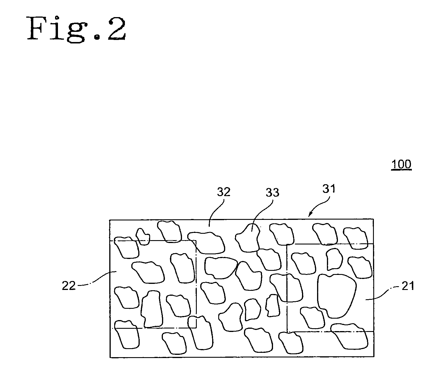
[0044]The functional layer 51 is a composite in which the conductive inorganic material 33 (not shown) is discretely dispersed in the matrix of the insulating inorganic material 32 (not shown). In the present embodiment, the functional layer 51 is formed by sputtering a target containing the insulating inorganic material 32 (or simultaneously sputtering a target containing the insulating inorganic material 32 and a target containing the conductive inorganic material 33) on the insulating surface 11a of the insulating substrate 11 and / or on the electrodes 21 and 22 and then applying a voltage between the electrodes 21 a...

example 1

[0048]First, sputtering was used to form a metallic thin film made of Cu and having a thickness of 100 nm nearly all over the insulating surface 11a, which is one surface of the insulating substrate 11 (an NiZn ferrite substrate having a dielectric constant of 13 manufactured by TDK Corporation), as shown in FIG. 4. Photolithography was then used to etch the thus formed Cu thin film so as to form a pair of strip-shaped electrodes 21 and 22 facing but spaced apart from each other. The gap distance ΔG between the electrodes 21 and 22 was 3 μm.

[0049]Thereafter, sputtering was used to form the functional layer 31 on the insulating substrate 11 and on the electrodes 21 and 22 in the following procedure, as shown in FIG. 5:

[0050]First, sputtering was used to form an Au film on parts of the surface of the insulating substrate 11 on which the electrodes 21 and 22 were formed. As a result, a layer of the conductive inorganic material 33 in which the island-shaped Au thin films having a thick...


PUM

PropertyMeasurementUnit
thicknessaaaaaaaaaa
frequencyaaaaaaaaaa
resistivityaaaaaaaaaa

Abstract

An ESD protection device that has low capacitance, excellent discharge characteristics, and improved heat resistance and weather resistance is provided. A functional layer 31, which is a composite having a conductive inorganic material 33 discretely dispersed in a matrix of an insulating inorganic material 32, is disposed between electrodes 21 and 22 disposed on an insulating substrate 11 and facing but spaced apart from each other.

Description

BACKGROUND OF THE INVENTION[0001]1. Field of the Invention[0002]The present invention relates to an ESD protection device, and particularly to an ESD protection device useful when used in a high-speed transmission system or combined with a common mode filter.[0003]2. Description of the Related Art[0004]Miniaturization and sophistication of electronic apparatus have rapidly been advancing in recent years. Considerable increase in transmission speed (frequency higher than 1 GHz) and decrease in drive voltages have also been achieved, as represented by USB 2.0, S-ATA2, HDMI, and other high-speed transmission systems. In contrast, withstand voltages of electronic components used in electronic apparatus decrease as the electronic apparatus are reduced in size and the drive voltages are reduced in amplitude. An important technical challenge in this case is to protect electronic components from overvoltages represented by electrostatic pulses produced when the human body comes into contact...

Claims


Application Information

Patent Timeline
Patent Type & Authority Applications(United States)
IPC IPC(8): H02H9/04
CPCH01L23/60H01L27/0248Y10T428/257H01L2924/0002H01L2924/00H01C7/12H05F1/00
Inventor HIROBE, YASUHIROASAKURA, KENSAKUHITOMI, ATSUSHIURANO, TAKESHI
Owner TDK CORPARATION
Why Eureka
Try Eureka