Method for initializing ferroelectric memory device, ferroelectric memory device, and electronic equipment

a technology of ferroelectric memory and initialization method, which is applied in the direction of digital storage, semiconductor devices, instruments, etc., can solve the problems of insufficient measurement described in patent documents, inability to reduce the imprint that has already occurred in capacitors, and insufficient technology. to achieve the effect of reducing the effect of imprint phenomenon

Inactive Publication Date: 2010-02-04
SEIKO EPSON CORP
View PDF5 Cites 11 Cited by
  • Summary
  • Abstract
  • Description
  • Claims
  • Application Information

AI Technical Summary

Benefits of technology

[0012]In accordance with an advantage of some aspects of embodiments of the present invention, there is provided a method for initializing a ferroelectric memory device, which is capable of resetting imprint phenomenon of capacitors caused by past thermal history, and reducing effects of imprint phenomenon that may be caused by processing to be conducted later.
[0014]According to the method described above, by imprinting the upper electrode in the positive direction at a temperature higher than an operation guarantee temperature in advance, the upper electrode can be prevented from imprinting in the negative direction later in a use state. It is noted here that the imprinting in the negative direction means that the hysteresis loop shifts to the left (in the negative potential direction) when potentials impressed to the upper electrode are plotted along the axis of abscissas.
[0018](2) A ferroelectric memory device in accordance with an embodiment of the invention is a ferroelectric memory device that is initialized by the method for initializing a ferroelectric memory device described above. According to such a structure, the upper electrode is imprinted in the positive direction in advance such that the upper electrode can be prevented from imprinting in the negative direction later in a use state, whereby its device characteristics can be improved. For example, the operation margin (write operation margin, in particular) can be improved. Also, low voltage driving (low voltage writing, in particular) becomes possible.
[0021]Preferably, after an operation of the initialization circuit, a heat treatment may be conducted at a temperature higher than an operation guarantee temperature. In this manner, the upper electrode is imprinted in the positive direction at a temperature higher than the operation guarantee temperature in advance, whereby the upper electrode can be prevented from imprinting in the negative direction later in a use state.

Problems solved by technology

Such imprint phenomenon could lead to operation errors.
In particular, processing and examination at high temperature may often have to be conducted, the measure described in Patent Document is not sufficient.
According to the technology described in Patent Document 2, the cool down processing is conducted in advance in order to prevent imprint from occurring in steps to be conducted later, thereby setting data (value) stored in capacitors to a state that is neither “0” or “1.” However, this technology cannot reduce imprint that has already occurred in capacitors.

Method used


Image

  • Method for initializing ferroelectric memory device, ferroelectric memory device, and electronic equipment
  • Method for initializing ferroelectric memory device, ferroelectric memory device, and electronic equipment
  • Method for initializing ferroelectric memory device, ferroelectric memory device, and electronic equipment

Examples


embodiment 1

[0034]Structure and Operation of Ferroelectric Memory Device

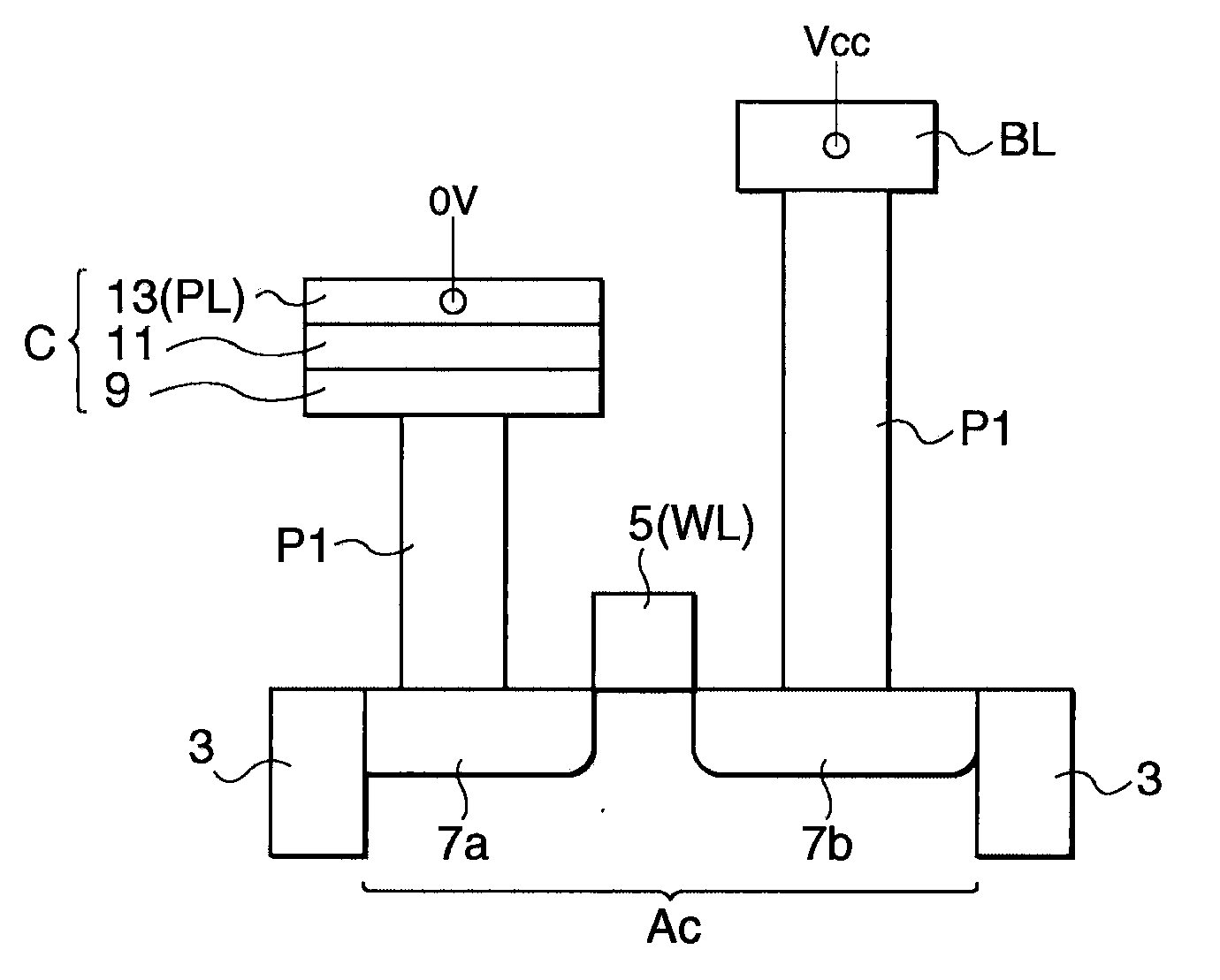
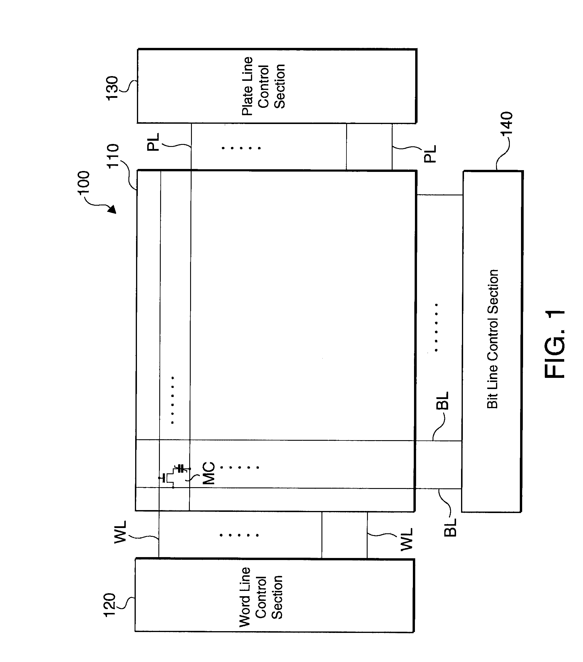
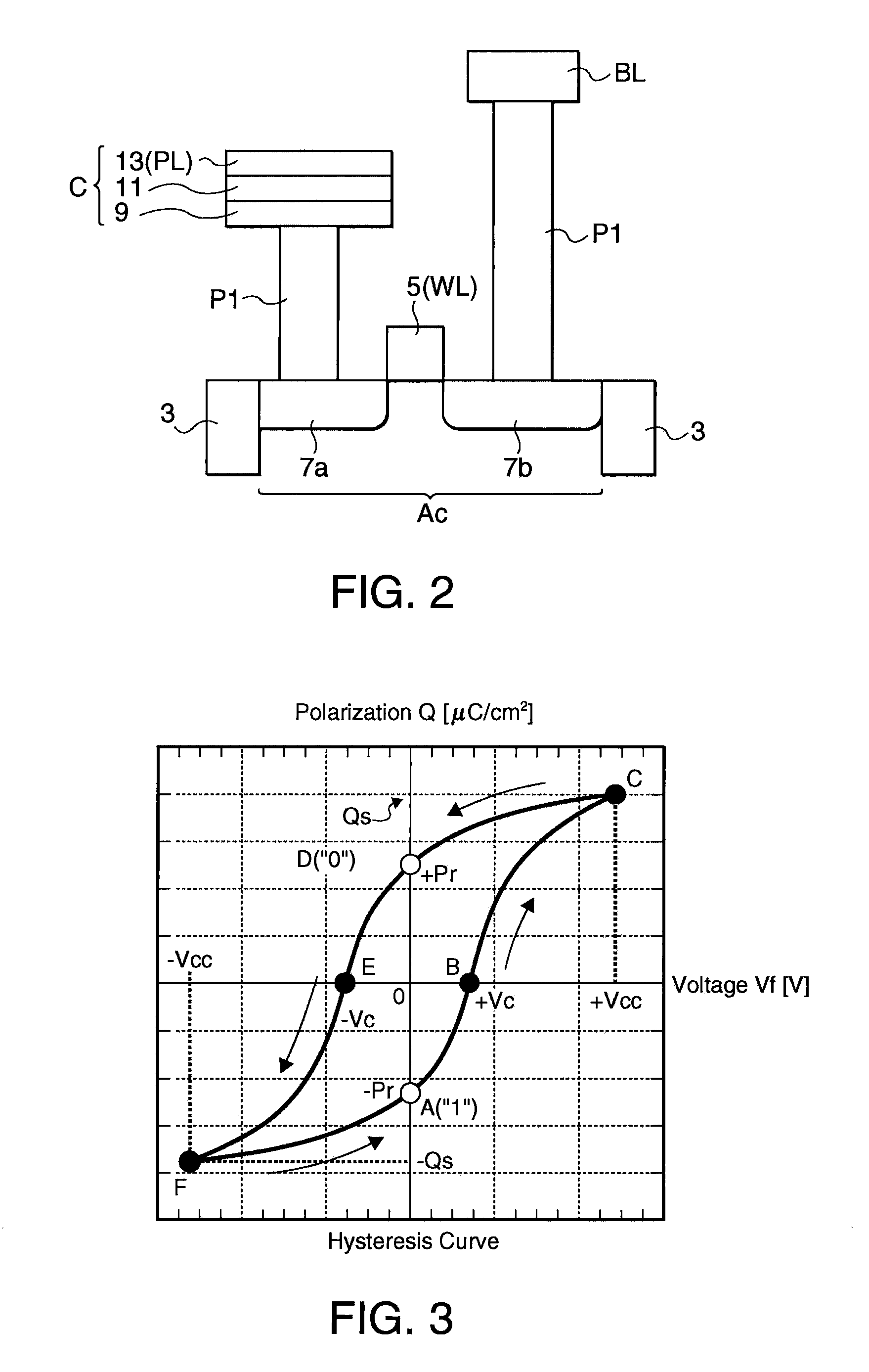
[0035]FIG. 1 is a block diagram of the structure of a ferroelectric memory device in accordance with an embodiment of the invention. As illustrated, the ferroelectric memory device 100 includes a memory cell array 110, and a peripheral circuit section (120, 130, 140, etc.). The memory cell array 110 is composed of a plurality of memory cells MC arranged in an array configuration, wherein each of the memory cells MC is disposed at an intersection between a word line WL and a bit line BL. In this embodiment, 1T1C cells are exemplified. In this case, each data is stored by a transistor and a ferroelectric capacitor connected in series between the bit line BL and the plate line PL. Also, a word line control section 120 and a plate line control section 130 which compose the peripheral circuit section control voltages on a plurality of word lines and a plurality of plate lines PL. Controlled by these circuits, data stored in the ...

embodiment 2

[0063]The embodiment 1 is described above, using a 1T1C type memory cell as an example. However, the invention is also applicable to 2T2C type memory cells.

[0064]FIG. 10 is a block diagram of a ferroelectric memory device in accordance with another embodiment of the invention. As shown in FIG. 10, in the case of a 2T2C type device, each data is stored by two transistors and two ferroelectric capacitors C1 and C2 respectively connected to bit lines BL and BLX.

[0065]At the time of writing, complementary data are written to the two ferroelectric capacitors C1 and C2 by a write amplifier WA. At the time of reading out, charges read out from those capacitors are compared and amplified by a sense amplifier SA, thereby judging whether the ferroelectric capacitors C1, C2 stored data “1” and “0” or stored data “0” and “1”. It is noted that, other than writing complementary data to the two ferroelectric capacitors C1 and C2 and reading from them, the structure and operations of the memory cel...


PUM


Abstract

A method for initializing a ferroelectric memory device is provided. The method includes the steps of: packaging a ferroelectric memory device having memory cells arranged in an array, each of the memory cells having a ferroelectric film disposed between a lower electrode and an upper electrode; applying a potential between the lower electrode and the upper electrode in an examination step; and after the examination step, applying a first potential to the upper electrode and applying a second voltage higher than the first potential to the lower electrode, and thereafter conducting a heat treatment at a first temperature higher than an operation guarantee temperature.

Description

[0001]The entire disclosure of Japanese Patent Application No. 2008-197993, filed Jul. 31, 2008 is expressly incorporated by reference herein.BACKGROUND[0002]1. Technical Field[0003]The present invention relates to technologies for initializing ferroelectric memory devices.[0004]2. Related Art[0005]A ferroelectric memory device (FeRAM: Ferroelectric Random Access Memory) is a memory device that uses the property (remnant polarization property) of a ferroelectric film in which the film is polarized by an externally applied electric filed, and the polarization remains even when the external electric field is removed. By changing the direction of electric field to be applied, the direction of polarization of ferroelectrics changes, whereby data can be rewritten.[0006]The ferroelectric film is required to have high film fatigue endurance, high retention property, small imprint phenomenon, and other various properties.[0007]Imprint is a phenomenon in which a polarization caused by applic...

Claims


Application Information

Patent Timeline
Patent Type & Authority Applications(United States)
IPC IPC(8): H01L29/00H01L21/00
CPCG11C11/22H01L27/11507G11C11/221H10B53/30
Inventor FUKADA, SHINICHI
Owner SEIKO EPSON CORP
Why Eureka
Try Eureka