Method for Manufacturing Vertical Germanium Detectors

a technology of germanium detectors and manufacturing methods, applied in the field of optical detectors, can solve the problems of limiting the application of such devices in the telecommunications industry, reducing the performance of devices, and high cost of silicon surface integration

Inactive Publication Date: 2010-02-04
BAE SYST INFORMATION & ELECTRONICS SYST INTERGRATION INC
View PDF13 Cites 10 Cited by
  • Summary
  • Abstract
  • Description
  • Claims
  • Application Information

AI Technical Summary

Problems solved by technology

However, the majority of the InGaAs-based detectors are normal incidence detectors, and the integration of such devices on silicon surfaces can be very expensive.
Also, integration of high-speed InGaAs detectors requires special optics to focus light into a small active area, which has been found to reduce device performance.
However, germanium-based detectors exhibit a higher dark current than InGaAs-based detectors, which limit their application in the telecommunications industry.

Method used


Image

  • Method for Manufacturing Vertical Germanium Detectors
  • Method for Manufacturing Vertical Germanium Detectors
  • Method for Manufacturing Vertical Germanium Detectors

Examples


Embodiment Construction

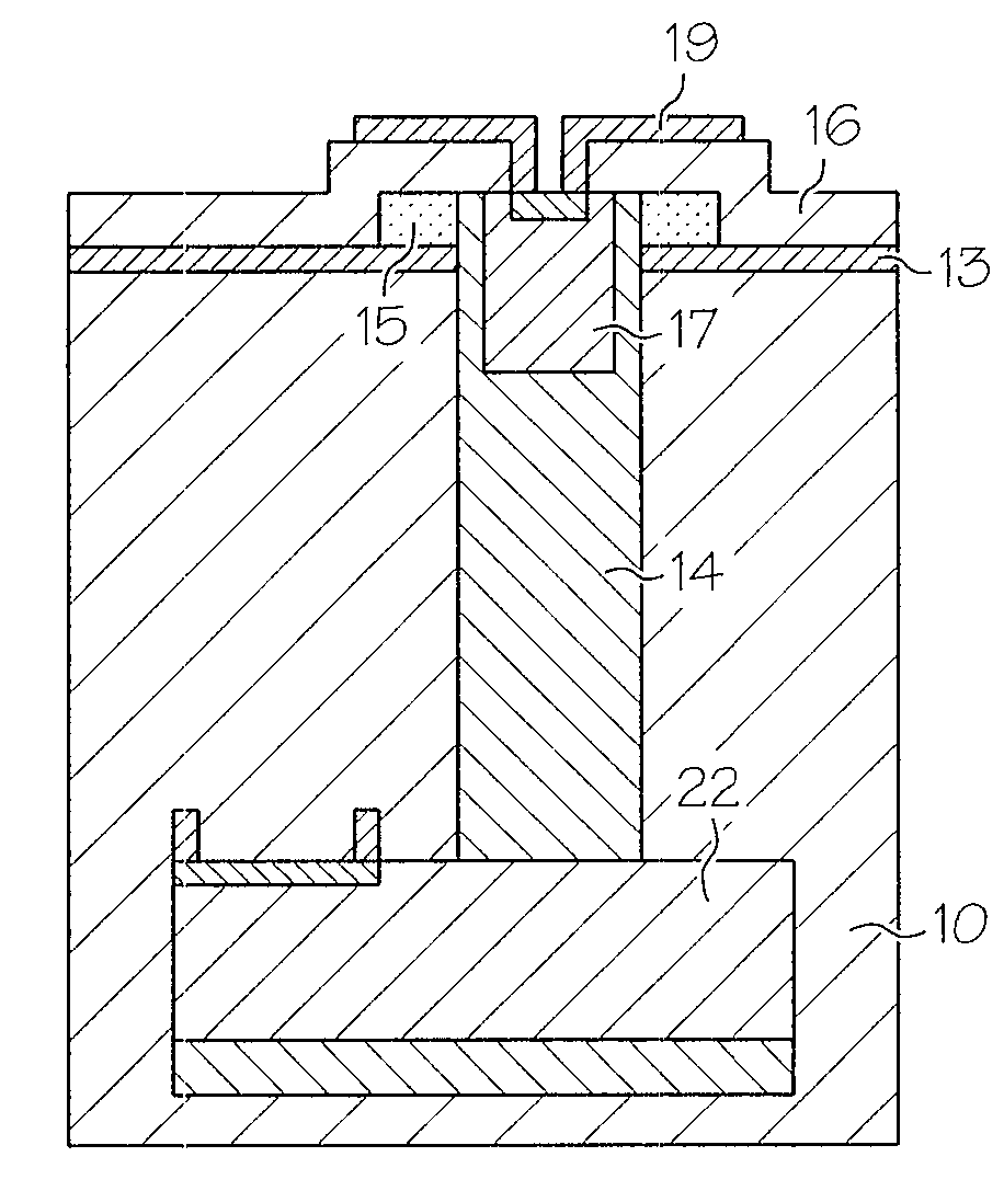
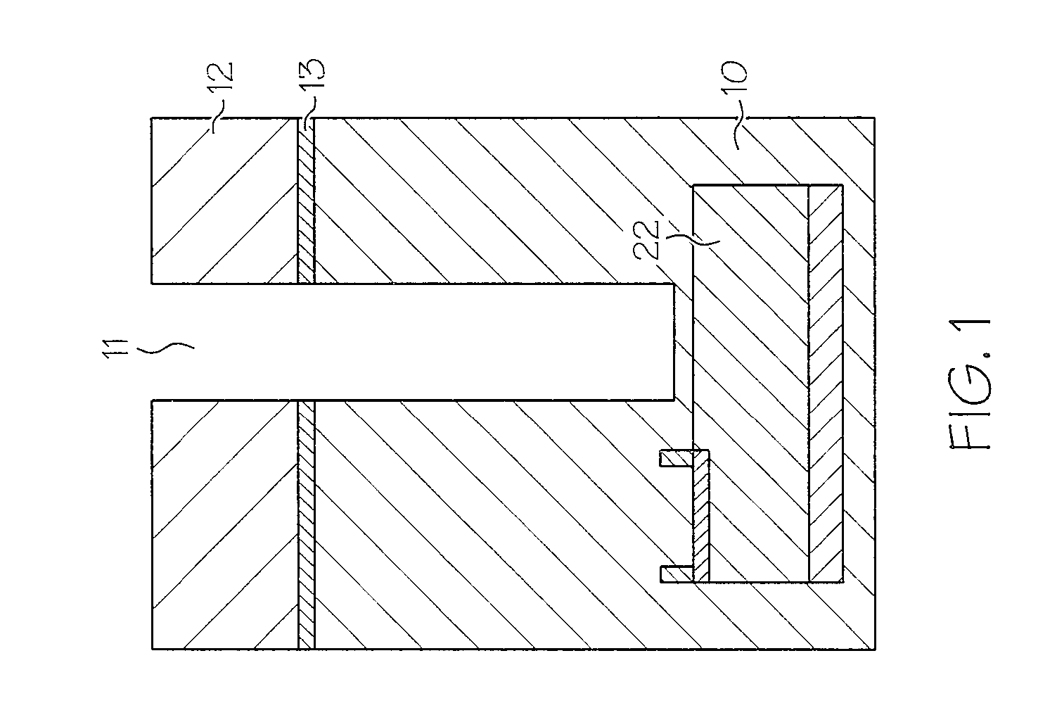
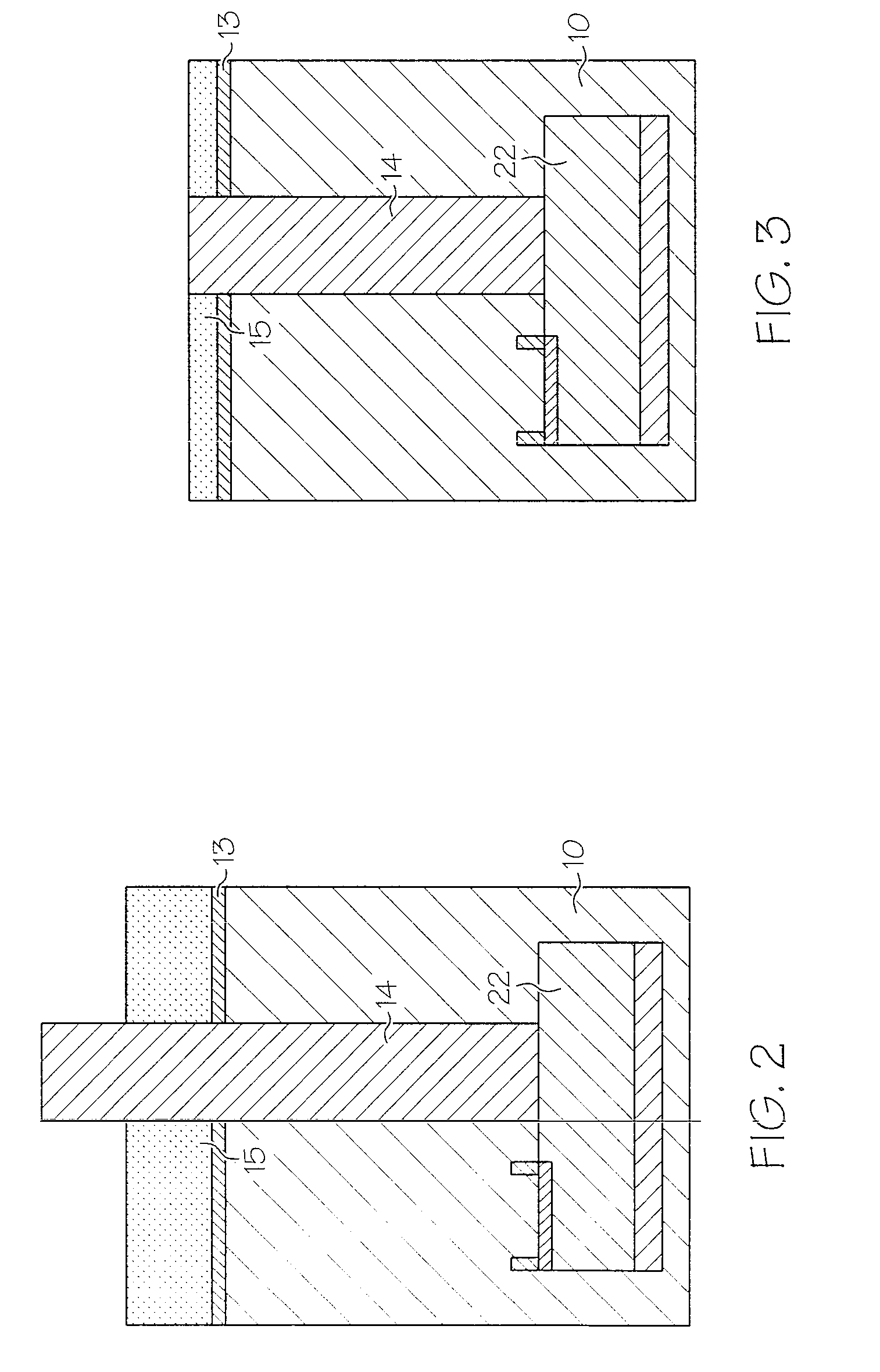
[0014]Referring now to the drawings and in particular to FIGS. 1-7, there are illustrated successive steps of a method for fabricating a vertical germanium-based detector, in accordance with a preferred embodiment of the present invention. Initially, a dry etch process is utilized to open a detector window 11 through a resist layer 12, a nitride layer 13 and an oxide layer 10 on an n+ doped single crystalline substrate having an implant 22 for detectors, as shown in FIG. 1.

[0015]A single crystal germanium layer 14 is then grown within detector window 11, as depicted in FIG. 2. The germanium growth process uses silicon and silicon-germanium seed layers to achieve an abrupt transition to the germanium growth by controlling the surface energy states that the germanium can adhere to as the germanium growth temperature is being modified. The usage of the seed layers allows for a subsequent single crystal germanium growth, even across very large exposed single crystal silicon regions. In ...


PUM


Abstract

An improved method for manufacturing a vertical germanium detector is disclosed. Initially, a detector window is opened through an oxide layer on a single crystalline substrate. Next, a single crystal germanium layer is grown within the detector window, and an amorphous germanium layer is grown on the oxide layer. The amorphous germanium layer is then polished and removed until only a portion of the amorphous germanium layer is located around the single crystal germanium layer. A tetraethyl orthosilicate (TEOS) layer is deposited on the amorphous germanium layer and the single crystal germanium layer. An implant is subsequently performed on the single crystal germanium layer. After an oxide window has been opened on the TEOS layer, a titanium layer is deposited on the single crystal germanium layer to form a vertical germanium detector.

Description

PRIORITY CLAIM[0001]The present application claims benefit of priority under 35 U.S.C. § 365 to the previously filed international patent application number PCT / US08 / 080471 filed on Oct. 20, 2008, assigned to the assignee of the present application, and having a priority date of Oct. 19, 2007, based upon U.S. provisional patent application No. 60 / 999,717, the contents of both applications are incorporated herein by reference.RELATED APPLICATION[0002]The present application is related to co-pending application Ser. No. 12 / 201,943 filed on Aug. 29, 2008, the contents of which are incorporated herein by reference.STATEMENT OF GOVERNMENT INTEREST[0003]The present invention was made with United States Government assistance under Contract No. HR0011-05-C-0027 awarded by Defense Advanced Research Projects Agency (DARPA). The United States Government has certain rights in the present invention.BACKGROUND OF THE INVENTION[0004]1. Technical Field[0005]The present invention relates to optical ...

Claims


Application Information

Patent Timeline
Patent Type & Authority Applications(United States)
IPC IPC(8): H01L31/0232
CPCH01L31/105Y02E10/50H01L31/1808H01L31/1055
Inventor CAROTHERS, DANIEL N.HILL, CRAIG M.POMERENE, ANDREW T.S.VU, VU A.GIUNTA, JOEISHII, JONATHAN N.
Owner BAE SYST INFORMATION & ELECTRONICS SYST INTERGRATION INC
Why Eureka
Try Eureka