Chemical vapor deposition method and system for semiconductor devices

a technology of chemical vapor deposition and semiconductor devices, which is applied in the direction of sustainable manufacturing/processing, final product manufacturing, coatings, etc., can solve the problems of difficult to achieve electric power generation using silicon-based solar cells, difficult to achieve parity, and high material and manufacturing costs of such solar cells

Inactive Publication Date: 2010-02-11
INT SOLAR ELECTRIC TECH INC
View PDF2 Cites 6 Cited by
  • Summary
  • Abstract
  • Description
  • Claims
  • Application Information

AI Technical Summary

Benefits of technology

[0009]The chemical vapor for deposition at each of the regions may cover an area greater than or equal to about 81 in2 (523 cm2), each of the substrates may have an area for the deposition of greater than or equal to that size, and the deposited layers of material may have a thickness of greater than or equal to about 0.1 micrometer (0.0039 mil) and less than or equal to about 3.0 micrometer (0.12 mil).
[0010]The pressure at the deposition surface of each of the plurality of substrates at the deposition regions may be greater than equal to about 0.5 torr and less than or equal to about 2.5 torr, and the temperature at the deposition surface of each of the plurality substrates at the deposition regions may be greater than or equal to about 100° C. and less than or equal to about 450° C.
[0011]The chemical vapor may include an organometallic material, such as diethyl zinc vapor (Zn(C2H5)2) or dimethyl zinc vapor (Zn(CH3)2). The chemical vapor may also include materials such as water vapor (H2O), nitrous oxide gas (NO), or hydrogen sulfide gas (H2S). Also, the atmosphere for the chemical vapor for one or more of the regions may include a material that provides a dopant for the layers, such as boron. Thus, the layers of material may include zinc oxide doped with boron.

Problems solved by technology

However, the material and manufacturing costs of such solar cells are relatively high.
Therefore, it is very difficult to achieve parity in electric power generation using silicon-based solar cells, in comparison to costs related to traditional sources of electrical energy.
More specifically, the manufacturing of large area thin film solar cells, with a required conversion efficiency, in a cost effective way, has proven an extremely great challenge.
The challenge for a layer such as this, as for a number of other formed layers, is the need to control its composition, its electronic and optical properties and its uniformity, over a large area substrate, while maintaining a significant rate of production.
However, the ceramic ZnO material targets used in this sputtering process are quite expensive, and the deposition rates for the ZnO material layers are quite low.
Thus, to achieve desired production rates, typically, a large number of ZnO material targets are required, making the sputtering system relatively large and expensive.
Each of these has been of limited usefulness.

Method used


Image

  • Chemical vapor deposition method and system for semiconductor devices
  • Chemical vapor deposition method and system for semiconductor devices
  • Chemical vapor deposition method and system for semiconductor devices

Examples


Embodiment Construction

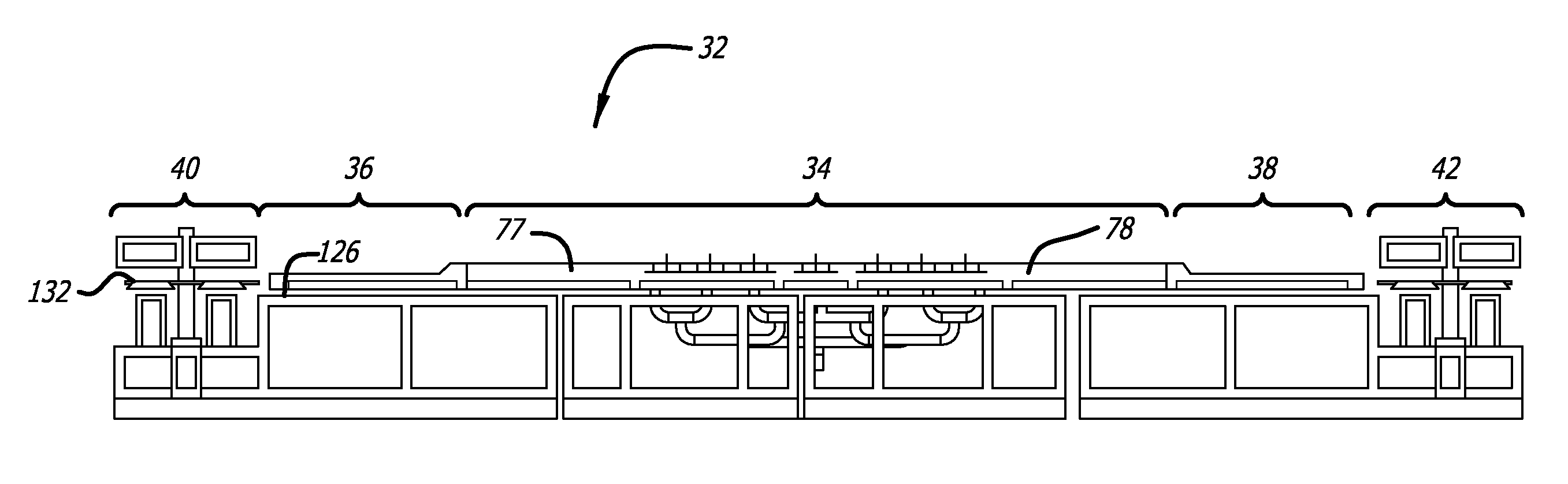
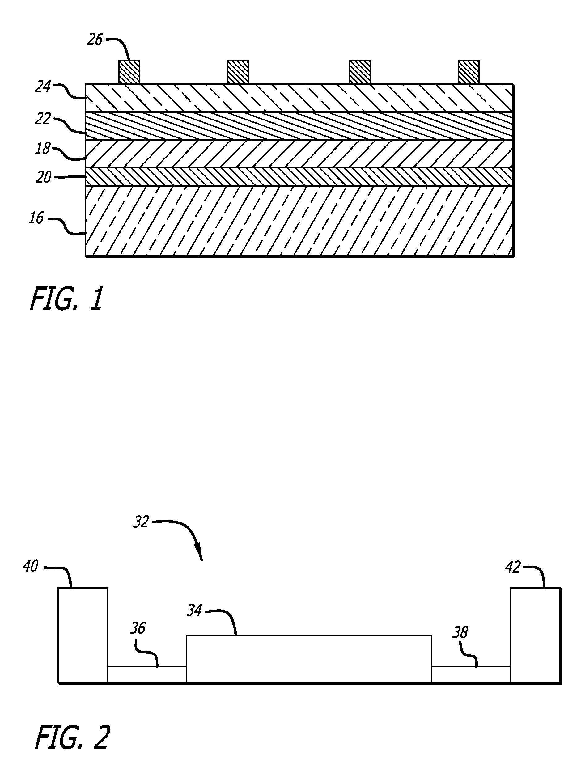
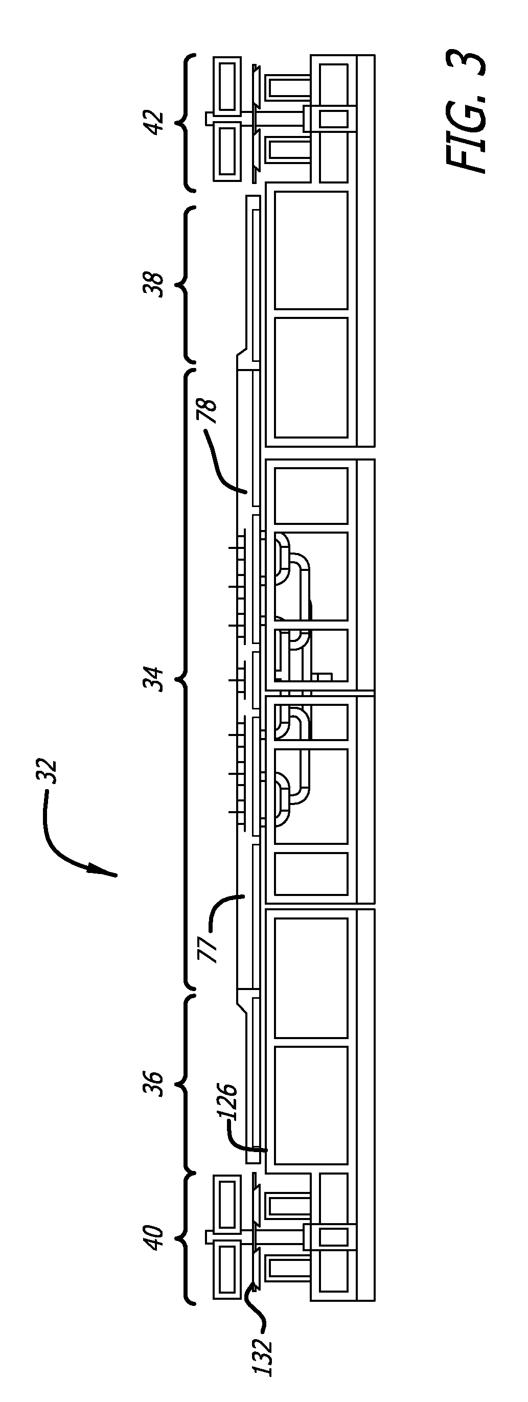
[0029]A typical general structure of a thin film solar cell, as well as one that may be made by using the method and system of the present invention, is shown in FIG. 1. The device is fabricated on a base that includes a sub-layer 16, that may typically be made, as shown, of a glass material, or alternatively of other material, such as a polymer, a suitable ceramic material, or a metal foil. A p-type absorber film 18 is deposited over a conductive layer 20, e.g., a metallic layer made of molybdenum (Mo), which acts as the back ohmic contact to the solar cell, and which is a coating for the sub-layer of the base. The sub-layer 16 and its coating 20, thus, may together be regarded as a base.

[0030]An n-type film 22 is formed on the p-type film. This, of course, forms a p-n junction that is critical to the performance of such a solar cell. Then, a window layer 24, generally transparent to the solar radiation of concern, is formed, through which radiation enters the device. The solar cel...


PUM

PropertyMeasurementUnit
thicknessesaaaaaaaaaa

Abstract

A method of and system for chemical vapor deposition of layers of material on substrates for producing thin film semiconductor devices provides for continuous in-line processing. The method and system are adapted for size and potential speed, and for scaling to further increase the rate of production. The method includes continuously conveying a plurality of substrates through a plurality of in-line deposition regions, continuously providing and distributing a chemical vapor at each region to deposit material for the layer, and continuously supplying a flow of chemical material for each region to provide the chemical vapor. The chemical vapor for deposition at each region covers an area that is substantial for substrates, then, also having a substantial area. The chemical vapor may include an organometallic material, such as diethyl zinc vapor, or dimethyl zinc vapor, as well as a material that provides oxygen, such as water vapor or nitrous oxide gas. It may also include a material that provides a dopant. Thus, the layers of material may be a zinc oxide material. The system includes a continuous in-line substrate conveyance apparatus for moving a plurality of substrates through a plurality of deposition regions, a deposition head for providing and distributing a chemical vapor at each of the regions to deposit material for the layers, and a chemical material supply apparatus for providing a flow of chemical materials to each of the heads for the chemical vapor. The chemical vapor deposition head includes an emission and distribution face at the region for the head, and wall structure defining a first plenum layer having a first plenum and a second plenum layer having a second plenum, for receiving chemical materials from the supply apparatus and for maintaining separation of received chemical materials. The head also includes wall structure defining a third plenum layer having a first set of elongated plenums for receiving chemical material from the first plenum and distributing such chemical material to the emission and distribution face, and a second set of elongated plenums for receiving chemical material from the second plenum and distributing such chemical material to the emission and distribution face. One exemplary number of deposition regions is seven.

Description

FIELD OF THE INVENTION[0001]This invention relates to methods and systems for the chemical vapor deposition of layers of material on substrates, and in particular, such deposition for producing semiconductor devices.BACKGROUND OF THE INVENTION[0002]Solar cells, of course, are semiconductor devices that have been the subject of substantial developmental effort over the years, including among many other aspects, improving their conversion efficiency and improving the methods and apparatus for producing solar cells at lower cost. These efforts have only been enhanced in recent years, with great concern and emphasis on attempting to progress toward parity in the cost of electricity generation by solar cells with traditional sources of electric power generation.[0003]The use of silicon-based semiconductor material for solar cells has an extended history. However, the material and manufacturing costs of such solar cells are relatively high. Therefore, it is very difficult to achieve parit...

Claims


Application Information

Patent Timeline
Patent Type & Authority Applications(United States)
IPC IPC(8): H01L21/3205C23C16/54
CPCC23C16/407C23C16/45574C23C16/54H01L31/022466Y02E10/541H01L31/0322H01L31/0749H01L31/1884H01L31/0296Y02P70/50
Inventor KAPUR, VIJAY K.KEMMERLE, RICHARD T.LE, PHUCAN
Owner INT SOLAR ELECTRIC TECH INC
Why Eureka
Try Eureka