Printed circuit board

a technology of printed circuit boards and circuit boards, applied in the direction of cross-talk/noise/interference reduction, electrical apparatus construction details, etc., can solve the problems of lsi power source or ground potential changes, erroneous operation of an lsi, signal output timing changes, etc., and achieve the effect of inexpensive configuration

Active Publication Date: 2010-02-18
CANON KK
View PDF5 Cites 17 Cited by
  • Summary
  • Abstract
  • Description
  • Claims
  • Application Information

AI Technical Summary

Benefits of technology

[0013]It is accordingly an object of the present invention to provide a printed circuit board designed such that radiation noise caused by a common mode noise arising from between the ground and the power source of a semiconductor integrated circuit mounted on a printed wiring board is reduced by an inexpensive configuration.

Problems solved by technology

Due to recent further increases in integration and processing speed of LSI (Large-Scale Integration), problems caused by changes in LSI power sources or ground potential have been increasing.
At the instant when this switching from the low to high level takes place, the charges are released from a power source conductor and a spike noise consequently occurs such that the power source potential momentarily decreases.
Such changes in potential cause, for example, erroneous operations of an LSI or changes in output timing of a signal.
However, a bypass capacitor disposed on a printed wiring board only reduces the noise arising from the differential between the power source and ground.
It is actually difficult to ensure an ideal ground and hence impossible to suppress a common mode noise in which the potentials of the power source and ground change in the same phase even when the bypass capacitor is used.
Like the differential mode noise, the common mode noise is emitted into the space, with a power source conductor and ground conductor as antennas, and increase radiation noise becomes increase radiation noise.
In addition, since the ferrite core is of a sintered body, it is difficult to produce small ferrite cores.
Accordingly, this is not an effective means in terms of cost either.
However, this technique is designed to reduce a common mode noise relative to differential signals, and cannot cope with a common mode noise arising from the power source and ground of a DC circuit.
It is known that such common mode noise arising between the power source and ground may cause considerable radiation noise even with slight current.

Method used


Image

  • Printed circuit board
  • Printed circuit board
  • Printed circuit board

Examples


first embodiment

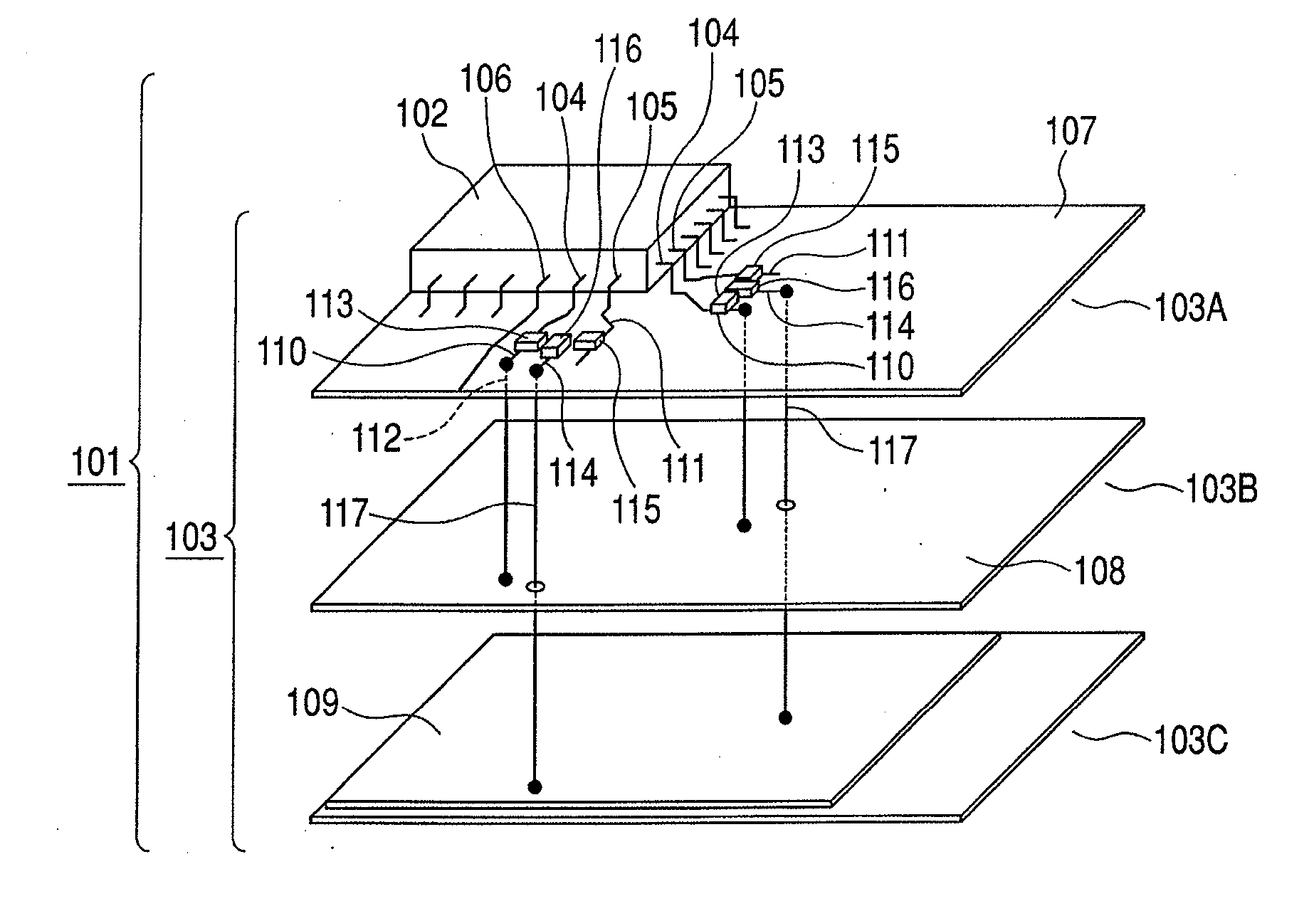
[0034]FIG. 1 is a schematic view of a printed circuit board according to a first embodiment. FIG. 2 is a plan view of the main part of the printed circuit board shown in FIG. 1, and shows in detail the part on which a power source terminal 104 and a ground terminal 105 of a semiconductor integrated circuit 102 are mounted.

[0035]The printed circuit board 101 includes the packaged semiconductor integrated circuit 102 and a multilayer printed wiring board 103. The semiconductor integrated circuit 102 in a QFP (Quad Flat Package) has the above-mentioned power source terminal 104, the ground terminal 105, and a plurality of signal terminals 106. The printed wiring board 103 is a multilayer (two-layer) board made of FR4. A first layer 103A has a ground plane 107. A second layer 103B has a power source plane 108 that supplies a reference potential. A third layer 103C has a plane conductor 109 that is not connected to the power source plane 108 and ground plane 107 directly. The printed wir...

second embodiment

[0044]FIG. 4 is a schematic view of the main part of a printed circuit board according to the second embodiment.

[0045]A printed circuit board 201 includes a semiconductor circuit 202 and a multilayer printed wiring board 203. The semiconductor integrated circuit 202 contained in a BGA (Ball Grid Allay) has a power source solder ball 204, a ground solder ball 205, and a plurality of signal solder balls 206. The printed wiring board 203 is a four-layer board made of FR4. The first layer 203A has a ground plane 207. The second layer 203B has a power source plane 208 that supplies reference potential. The third layer 203C has a plane conductor 209 that is not connected to the power source plane 208 and ground plane 207 directly. The fourth layer 203D forms the back of the printed wiring board 203, and various electronic components are mounted on this back.

[0046]Perspectively viewing the printed circuit board 201 from a vertical direction, it is preferable that the area of the plane cond...

third embodiment

[0052]FIG. 6 is a perspective view of a printed circuit board according to a third embodiment. FIG. 7 is a graph representing the radiation noise reduction effect in the third embodiment.

[0053]The printed circuit board 301 includes a semiconductor integrated circuit 302, a first printed wiring board 303 and a second printed wiring board 304. The semiconductor integrated circuit 302 and the first printed wiring board 303 are electrically and physically connected by a bonding wire 305 and covered by a resin mold 306. The first printed wiring board 303 and the second printed wiring board 304 are connected by a power source solder ball 319 and a ground solder ball 321.

[0054]The power source of the semiconductor circuit 302 and the power source pattern 309 of the first printed wiring board 303 are connected by a power source bonding wire 307. The ground of the semiconductor integrated circuit 302 and the ground pattern 310 of the first printed wiring board 303 are connected by a ground b...


PUM


Abstract

A power source terminal and a ground terminal for a semiconductor integrated circuit are connected to a conductor pattern through a capacitor. The conductor pattern is connected, through a filter, to a plane conductor connected to neither a ground plane nor a power source plane. Thus, a common mode noise arising from between the power source and the ground is caused to flow into the plane conductor. This reduces the common mode noise flowing in the ground and the power source of the printed wiring board, which relatively act as antennas.

Description

TECHNICAL FIELD[0001]The present invention relates to printed circuit boards in which a semiconductor element such as an LSI is mounted on a printed wiring board.BACKGROUND ART[0002]Due to recent further increases in integration and processing speed of LSI (Large-Scale Integration), problems caused by changes in LSI power sources or ground potential have been increasing. In order for an LSI circuit to be operated, a power source for applying a high potential and a ground for applying a low potential are required.[0003]FIGS. 13A and 13B are diagrams illustrating the relation between an inverter circuit of a CMOS, its signal output, and a change in power source and ground potential. When the output of the CMOS inverter configured as shown in FIG. 13A switches from a low level to a high level, the NMOS 805 side is closed and the PMOS 804 side is opened. Consequently, charging current 807 is produced such that charges accumulated in a power source 802 pass through the PMOS 804 and accum...

Claims


Application Information

Patent Timeline
Patent Type & Authority Applications(United States)
IPC IPC(8): H05K1/18H05K1/02
CPCH05K1/0231H05K1/0233H05K1/0234H05K2201/09309H05K2201/09336H05K2201/10734H05K2201/10022H05K2201/1003H05K2201/10522H05K2201/10545H05K2201/10689H05K2201/09781H01L2224/48091H01L2224/49171H01L2924/15311H01L2924/19105H05K1/0298H01L2924/00014H05K1/02H05K3/46
Inventor HAYASHI, SEIJI
Owner CANON KK
Why Eureka
Try Eureka