Non-volatile programmable optical element employing f-centers

Active Publication Date: 2010-02-18
GLOBALFOUNDRIES US INC
View PDF7 Cites 11 Cited by
  • Summary
  • Abstract
  • Description
  • Claims
  • Application Information

AI Technical Summary

Benefits of technology

[0011]In the present invention, a non-volatile programmable electro-optical element alters absorption characteristics of an optical medium that comprises a doped transition metal oxide material including F-centers. The F-centers are electrostatically moved into or out of the regions containing a wavefunction of an optical beam. A specific F-center profile in the transition metal oxide material may be programmed into the optical medium. The F-center profile alters an absorption profile within the optical medium. The spectral range for transmission of electromagnetic radiation in the opti

Problems solved by technology

The main drawback of the above-mentioned electro-optical elements employing a semiconductor material is “volatility” of the change in the absorption characteristics of the semiconductor material.
Such electro-optical elements are “volatile,” i.e., they do not maintain the characteristics of a programmed state once power to the electro-optical element is turned off.
A further disadvantage of the prior art optical elements employing a semiconductor material is that such electro-optical elements typically employ silicon or germanium, and are thus only suitable for the infrared wavelength range.
The main drawback of the above-mentioned electro-optical elements employing a ferromagnetic perovskite material is that these elements are only suitable for the far-infrared wavelength region.
Specifically, such electro-

Method used


Image

  • Non-volatile programmable optical element employing f-centers
  • Non-volatile programmable optical element employing f-centers
  • Non-volatile programmable optical element employing f-centers

Examples


second embodiment

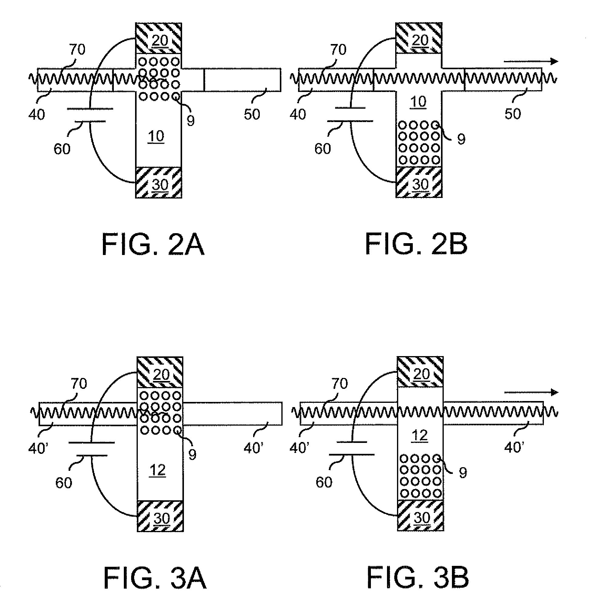
[0075]Referring to FIGS. 3A and 3B, a second exemplary electro-optical structure is shown in see-through top-down views according to the present invention. The second exemplary electro-optical structure employs a doped transition metal oxide structure 12 that is distinct from an optical medium structure (not shown) that underlies a doped transition metal oxide structure 12. FIG. 3A shows the second exemplary electro-optical structure in a first switching state in which a doped substantially stoichiometric transition metal oxide region including F-centers 9 overlies a path of electromagnetic radiation 70. FIG. 3B shows the second exemplary electro-optical structure in a second switching state in which a doped oxygen-deficient transition metal oxide region substantially free of F-centers 9 overlies or underlies the path of the electromagnetic radiation 70.

[0076]While the second exemplary electro-optical structure employs an optical medium structure that underlies the doped transition ...

first embodiment

[0077]The second exemplary electro-optical structure comprises the doped transition metal oxide structure 12, the optical medium structure that underlies the doped transition metal oxide structure and aligned to a waveguiding structure 40′, a first electrode 20 and a second electrode. The optical medium structure may comprise a waveguide core, and the doped transition metal oxide structure 12 may comprise a waveguide cladding, i.e., a layer that abuts, surrounds, or encloses the surfaces of the waveguide core. The F-centers move between the first electrode 20 and the second electrode 30 in the same manner as in the Electromagnetic radiation 70 passes through the waveguiding structure 40′ and into the doped transition metal oxide structure 12 because the wavefunction of the electromagnetic radiation extends outside of the waveguiding structure 40′ into the doped transition metal oxide structure 12 with an exponential decay in magnitude with distance from the surface of the optical m...

sixth embodiment

[0090]FIGS. 7A and 7B are cross-sectional views of a sixth exemplary electro-optical device according to the present invention. FIG. 7A is a cross-sectional view of the sixth exemplary electro-optical device in a first switching state, and FIG. 7B is a cross-sectional view of the sixth exemplary electro-optical device in a second switching state. The sixth exemplary electro-optical device comprises an optical switch including a doped transition metal oxide structure 10, a first electrode 20, and a second electrode 30. The optical switch (10, 20, 30) may be substantially the same as the assembly of the doped transition metal oxide structure 10, the first electrode 20, and the second electrode 30 in the first exemplary electro-optical structure described above. The sixth exemplary electro-optical structure further comprises a light source 380 and a screen element 390. The sixth exemplary electro-optical device may be employed as a display element, in which electromagnetic radiation 70...


PUM


Abstract

A non-volatile programmable electro-optical element alters absorption characteristics of an optical medium that comprises a doped transition metal oxide material including F-centers. The F-centers are electrostatically moved into or out of the regions containing a wavefunction of an optical beam. A specific F-center profile in the transition metal oxide material may be programmed into the optical medium. The F-center profile alters an absorption profile within the optical medium. The spectral range for transmission of electromagnetic radiation in the optical medium may be tailored by the F-centers. Once the absorption profile is set by an electrical signal, the optical element maintains its state even when the electrical signal is turned off. Thus, the programming node may be disconnected from a power supply network, thereby enabling a low power operation of the electro-optical element. The inventive electro-optical element may be employed for both the visible and the infrared wavelength spectrum.

Description

RELATED APPLICATIONS[0001]The present application is related to co-assigned and co-pending U.S. application Ser. No. ______ (Attorney Docket No: CH920080071US1; SSMP 22818), which is incorporated herein by reference.FIELD OF THE INVENTION[0002]The present invention relates to an optical structure, and particularly to a non-volatile programmable optical element that modulates the absorption coefficient of an optical material with F-center, methods of manufacturing the same, and methods of operating the same.BACKGROUND OF THE INVENTION[0003]Optical devices such as optical modulators or displays employ electro-optical elements that rely on modification of light absorption induced by an electrical signal. For example, U.S. Pat. Nos. 3,854,795, 5,016,990, and 7,016,094 provide electro-optical devices such as switches, filters, and tunable lasers, which are characterized by the modification of an absorption coefficient induced by an electrical-signal. Electrical-signal induced modificatio...

Claims


Application Information

Patent Timeline
IPC IPC(8): G11C11/34H01L21/02
CPCG02F1/011G02F1/1523G02F2203/15G02F1/313G02F3/022G02F1/225
Inventor MEIJER, GERHARD I.STOFERLE, THILO H. C.
Owner GLOBALFOUNDRIES US INC
Why Eureka
Try Eureka