Composites and devices including nanoparticles
- Summary
- Abstract
- Description
- Claims
- Application Information
AI Technical Summary
Benefits of technology
Problems solved by technology
Method used
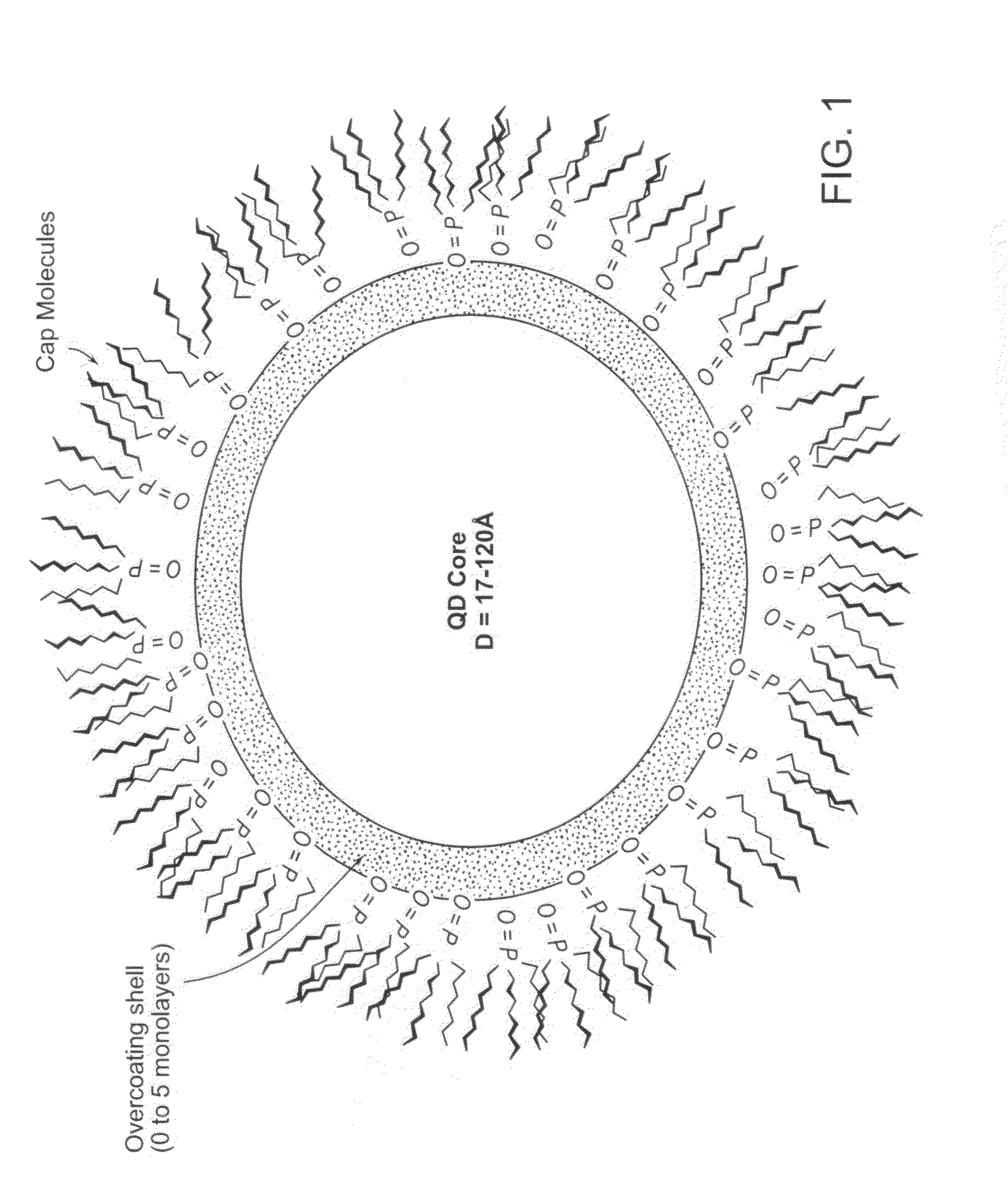
Image

Examples
example 1
Preparation of Aromatic Semiconductor Nanocrystals Capable of Emitting Red Light
[0116]Synthesis of CdSe Cores: 1 mmol cadmium acetate was dissolved in 8.96 mmol of tri-n-octylphosphine at 100° C. in a 20 mL vial and then dried and degassed for one hour. 15.5 mmol of trioctylphosphine oxide and 2 mmol of octadecylphosphonic acid were added to a 3-neck flask and dried and degassed at 140° C. for one hour. After degassing, the Cd solution was added to the oxide / acid flask and the mixture was heated to 270° C. under nitrogen. Once the temperature reached 270° C., 8 mmol of tri-n-butylphosphine was injected into the flask. The temperature was brought back to 270° C. where 1.1 mL of 1.5 M TBP-Se was then rapidly injected. The reaction mixture was heated at 270° C. for 15-30 minutes while aliquots of the solution were removed periodically in order to monitor the growth of the nanocrystals. Once the first absorption peak of the nanocrystals reached 565-575 nm, the reaction was stopped by co...
example 2
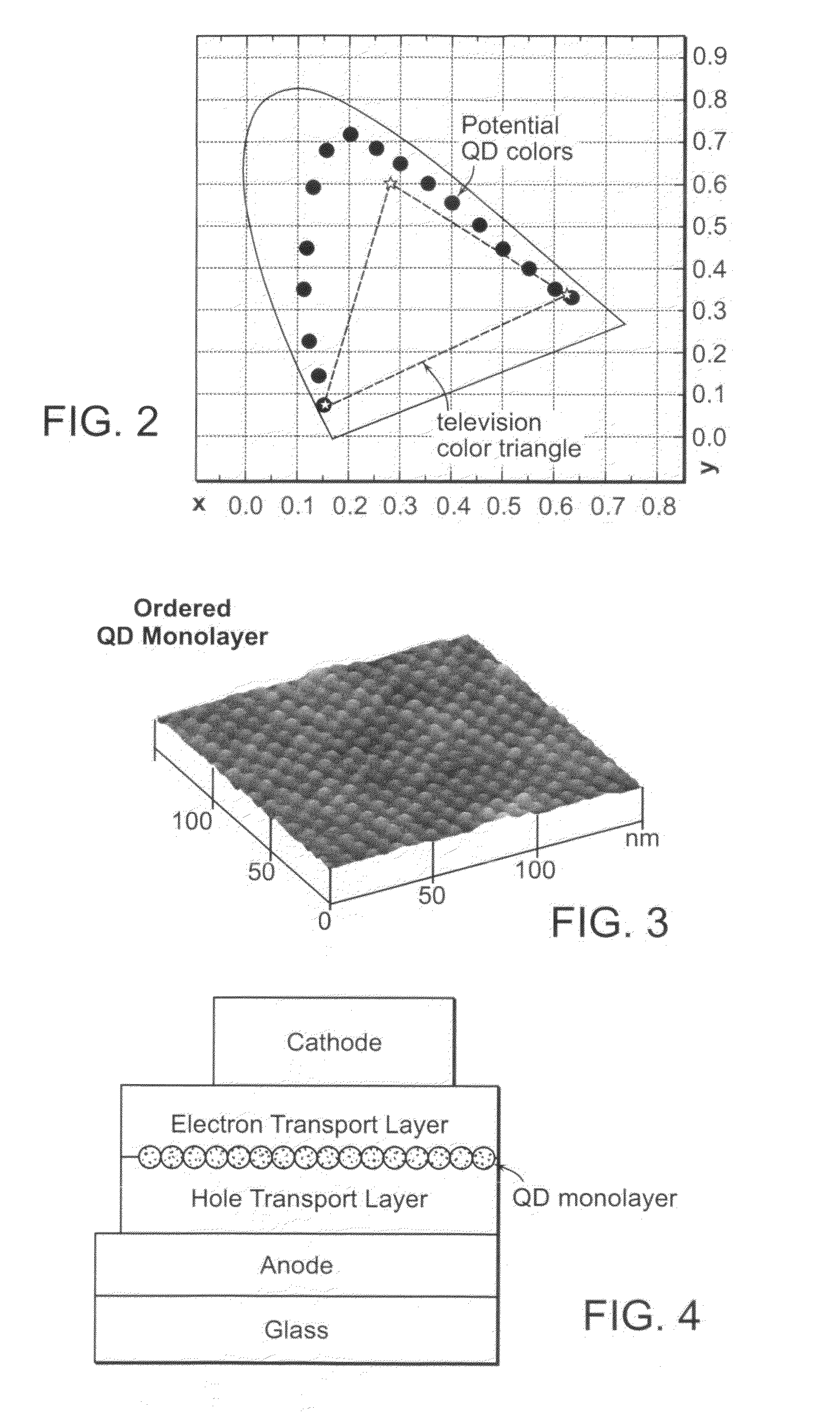
Sample Fabrication
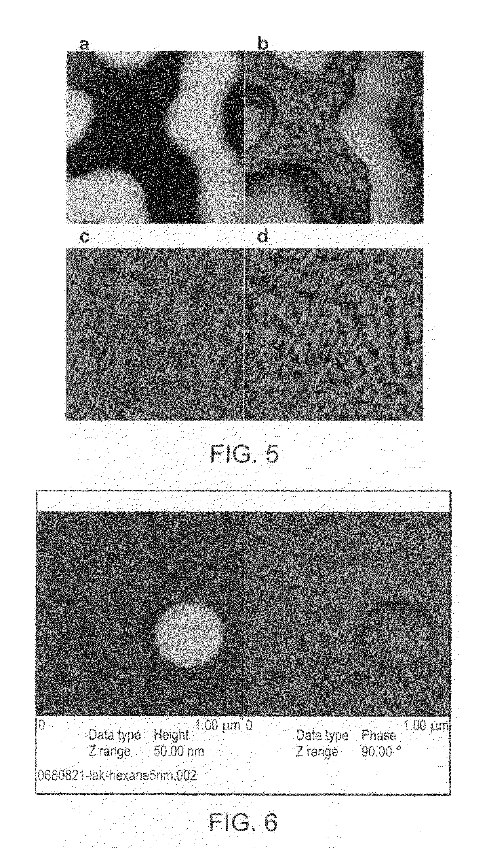
[0118]Cleaned glass substrates were ashed in a plasma preen and coated with PEDOT:PSS (70 nm). Substrates were taken into a nitrogen environment and baked at 120 C for 20 minutes. 50 nm E105 (N,N′-Bis(3-methylphenyl)-N,N′-bis-(phenyl)-9,9-spiro-bifluorene, LumTec) was evaporated in a vacuum chamber below 2e-6 Torr via thermal evaporation. Application of aromatic quantum dots was accomplished via contact printing. A dispersion of semiconductor nanocrystals with an optical density (OD) of 0.3 at the 1st absorption feature was spin-coated at 3000 rpm on a parylene coated stamp for 60 seconds, which was then stamped onto the E105 substrates depositing a mono-layer of aromatic quantum dots. Substrates were then taken back into the thermal evaporation chamber, and 5 nm and 15 nm, respectively, of CBP (4,4′-Bis(carbazol-9-yl)biphenyl, LumTec) were evaporated below 2e-6 Ton. FIG. 5(a)-(d) and FIG. 6-9 depict images of the samples described in this Example 2.
example 3
[0119]FIG. 11-12 show AFM images of additional examples of composites including a first layer comprising semiconductor nanocrystals including ligands with aromatic functionalities and a second layer comprising DOFL-CBP (2,7-Bis(9-carbazolyl)-9,9-dioctylfluorene). (DOFL-CBP is available from Luminescence Technology Corp., 2F, No. 21 R&D Road, Science-Based Industrial Park, Hsin-Chu, Taiwan, R.O.C., 30076.) The semiconductor nanocrystals in the depicted samples were prepared by a method similar to that described in Example 1, but in the absence of the amine species (phenylethylamine). FIG. 10 shows a layer of such semiconductor nanocrystals including ligands with aromatic functionalities on a glass substrate. FIG. 11 shows a layer of semiconductor nanocrystals similar to those shown in FIG. 10 with a 5 nm layer of DOFL-CBP formed on the nanocrystal layer. FIG. 12 shows a layer of semiconductor nanocrystals similar to those shown in FIG. 10 with a 15 nm layer of DOFL-CBP formed on the ...
PUM
 Abstract
Description
Claims
Application Information