
Fine-pattern structural body manufacturing method and fine-pattern structural body

Inactive Publication Date: 2010-03-18
NEC CORP
View PDF1 Cites 0 Cited by
  • Summary
  • Abstract
  • Description
  • Claims
  • Application Information

AI Technical Summary

Benefits of technology

[0024]The present invention has been designed in view of the aforementioned issues. It is therefore an exemplary object of the present invention to provide a fine-pattern structural body manufacturing method and the like, which provide advantages such as an excellent handling property.

Problems solved by technology

However, there are following issues with the related techniques described above.
However, it is extremely difficult to control the amount of the resin in such a small amount.
Therefore, it is not possible with the injection molding method to mold the film substrates of about 100 μm in thickness with a good regenerability.
When a part of the polytetrafluoroethylene film is exfoliated in this manner, that part turns out as a defect when transferring the pattern.
Thus, smooth separation cannot be expected at the time of mold release after transferring the pattern.
This makes the process thereof extremely complicated.
However, the above-described fluorine-based compound exhibits no sensitivity for the ultraviolet rays, so that it is necessary to apply a heat treatment after the drip feeding.
Thus, the forming steps become extremely complicated, and adjustment of the film thickness becomes difficult when vapor deposition is employed.
Furthermore, since it is necessary to apply the heat treatment at a high temperature of about 100 degrees C. for improving the contact property between the oxide thin film and the fluorine-based compound thin film described above, the original disk and the stamper to be used are required to have heat-resistance characteristic for the temperature of 100 degrees C. Therefore, it is difficult to use an organic-resin type material having a low-glass transition point, e.g., PC, with this process.
Moreover, a new issue has become apparent that when such process is conducted on an extremely thin film substrate of about 100 μm in thickness, the film substrate itself reacts to the adhesive accelerator, resulting in deformation and shrinkage.
However, it is found that there are followings issues with the pattern transferring method disclosed in Patent Document 4, With the thin-type optical disk fabricating method described above, positioning of the center hole of the film substrate formed in advance and the center hole of the stamper at the time of transferring the fine pattern of the stamper to the film substrate is determined only with the finished size accuracy of the center pole of the same diameter.
It is therefore found that the obtained thin-type optical disk is hard to record or reproduce information correctly.
It is found that such air bubbles exist as defects when transferring the pattern.
This deformation occurs in a state with an increase in the temperatures, so that it remains as a defect even after the structural body is exposed to the air after depositing the film.
It is therefore found that, as a result, the deformation influences the signal quality at the time of recording and reproduction, as the substrate defect of the thin-type optical disk.
Thus, those air bubbles under the decompression atmosphere can cause the defects.
Thus, it is hard to be handled at the time of external diameter processing.
Thus, it is found that there are increased numbers of defects generated due to deformations and breaks in the fine pattern and due to mixture of fine particles and the like at the time of laminating the cover sheet.

Method used


Image

  • Fine-pattern structural body manufacturing method and fine-pattern structural body
  • Fine-pattern structural body manufacturing method and fine-pattern structural body
  • Fine-pattern structural body manufacturing method and fine-pattern structural body

Examples


Embodiment Construction

[0056]In each exemplary embodiment described hereinafter, a transparent stamper on which an optical disk pre-format or lands / grooves are formed is used as a mold. For the transparent stamper, a stamper obtained by forming a pattern on quartz glass or a stamper obtained by forming a pattern on a PC (polycarbonate) substrate is used as appropriate. For a film substrate, a flexible PC film substrate of about 75 μm-120 μm in thickness, a PET (polyethylene terephthalate) film substrate, or an amorphous polyolefin film substrate is used as appropriate. Further, for the rigid substrate having rigidity, a PC substrate of 1.2 mm in thickness with a dummy groove manufactured in a large amount by injection molding is used. Furthermore, for each ultraviolet curing resin used in each exemplary embodiment, an ultraviolet curing resin from which bubbles are eliminated in vacuum before being applied is used. The bubbles are eliminated in vacuum in order to prevent micro bubbles that are rarely mixe...


PUM

PropertyMeasurementUnit
Thicknessaaaaaaaaaa
Pressureaaaaaaaaaa
Pressureaaaaaaaaaa

Abstract

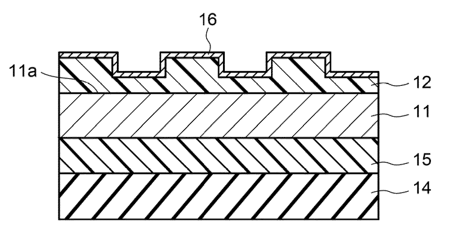
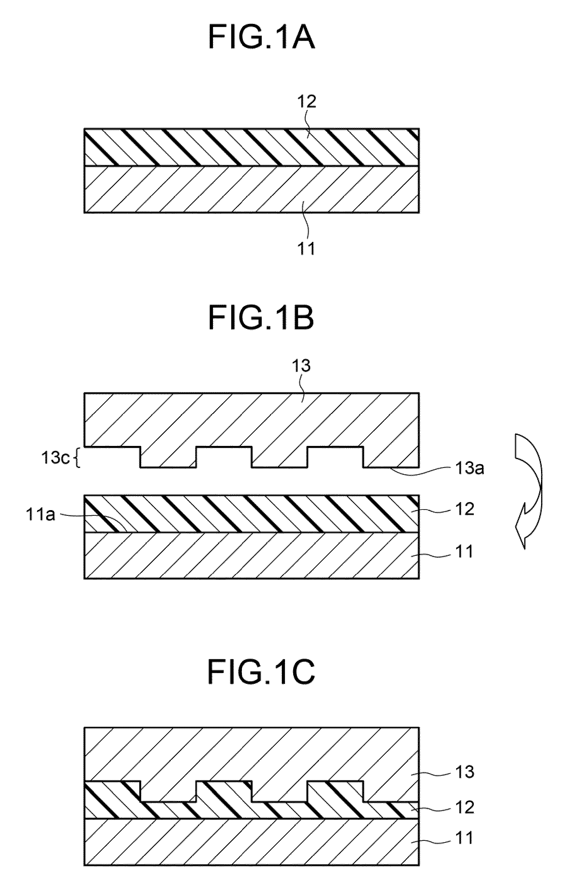
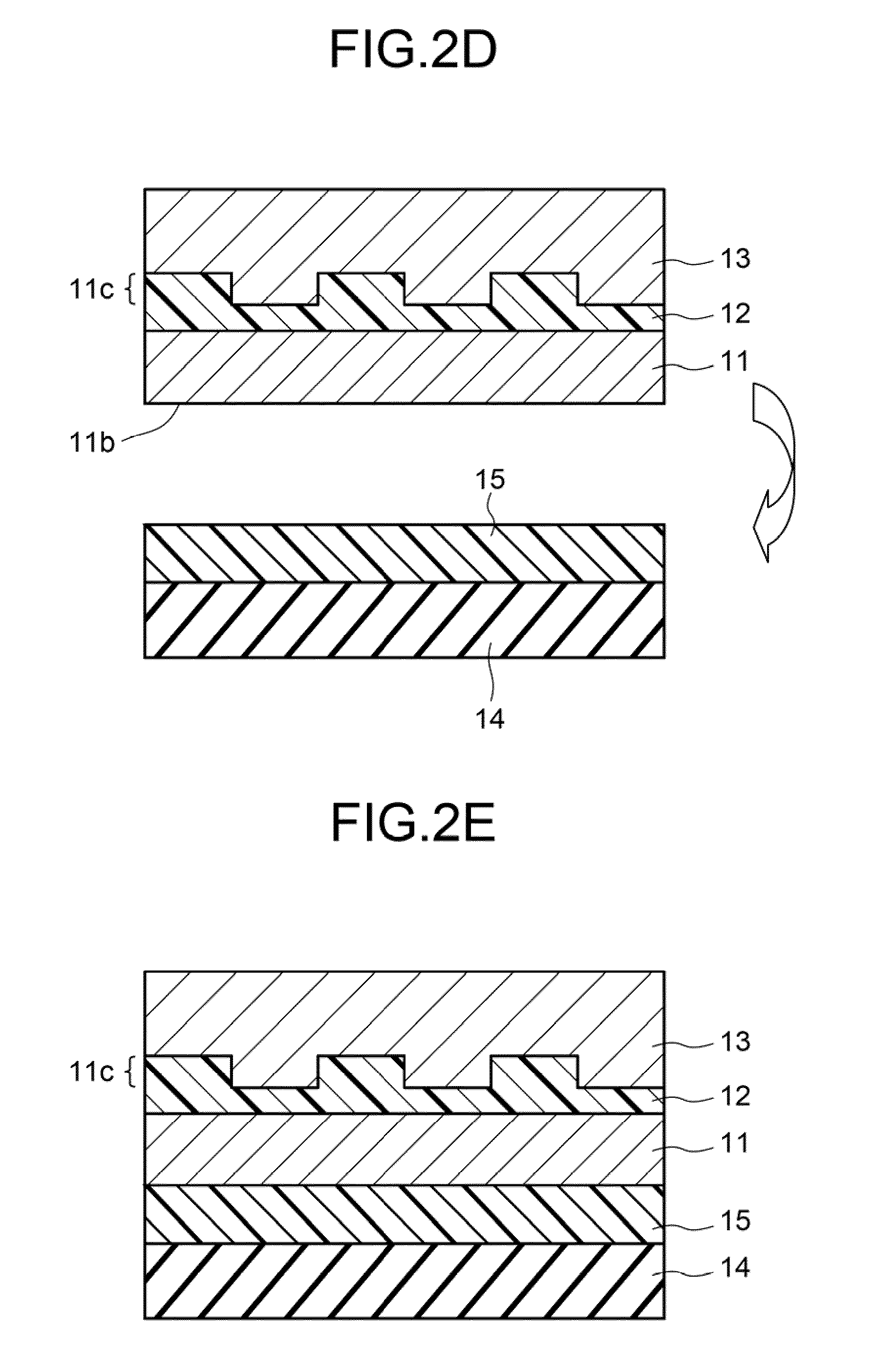
To provide a fine-pattern structural body manufacturing method having advantages such as excellent handling property. The fine-pattern structural body manufacturing method of the present invention includes following steps, i.e., a step of laminating a film substrate having flexibility and a mold having a fine pattern formed thereon in such a manner that one surface of the film substrate and a surface of the mold where the fine pattern is formed face with each other, a step of laminating other surface of the film substrate and a rigid substrate having rigidity, a step of separating the mold from the film substrate, a step of forming a recording film on the surface of the film substrate from which the mold is separated, a step of forming a protective film on the recording film, and a step of separating the rigid substrate from the film substrate.

Description

CROSS-REFERENCE TO RELATED APPLICATION[0001]This application is based upon and claims the benefit of priority from Japanese patent application No. 2008-236846, filed on Sep. 16, 2008, the disclosure of which is incorporated herein in its entirety by reference.BACKGROUND OF THE INVENTION[0002]1. Field of the Invention[0003]The present invention relates to a manufacturing method and the like of a fine-pattern structural body that is used when conducting micro-machining on storage devices, optical devices, bio devices, semiconductor devices, etc.[0004]2. Description of the Related Art[0005]In accordance with rapid developments in recent digital, information society, there has been a demand for implementing mass capacity in optical disks that are typical storage devices. Accordingly, developments of such disks have been conducted vigorously in various places. In currently-commercialized Φ120 mm optical disks, the pit length is 0.1 μm-0.2 μm and the capacity thereof is about 15 GB-30 GB....

Claims


Application Information

Patent Timeline
IPC IPC(8): B32B3/10B32B38/06
CPCB32B38/06B32B2429/02Y10T428/24802Y10T156/1039G11B7/263
Inventor KARIYADA, EIJI
Owner NEC CORP
Learn More