Opto-electronic device
- Summary
- Abstract
- Description
- Claims
- Application Information
AI Technical Summary
Benefits of technology
Problems solved by technology
Method used
Image

Examples
first embodiment
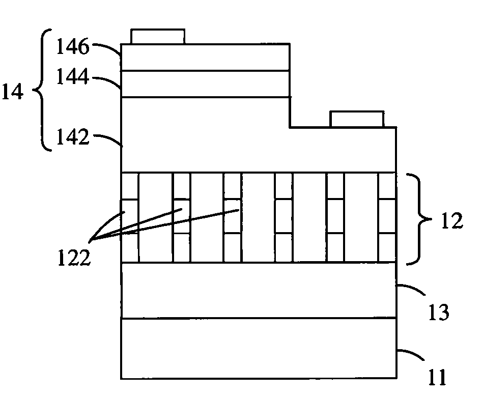
[0022]FIG. 1 is a schematic view of an opto-electronic device in accordance the present application. Referring to FIG. 1, the opto-electronic device 10 is a light-emitting diode, which includes a first light-emitting structure 12 and a second light-emitting structure 14. The first light-emitting structure 12 can emit a first light having a first wavelength. The second light-emitting structure 14 can emit a second light having a second wavelength. The first light-emitting structure 12 includes a nanorod structure having a first active layer 122 which can absorb the second light to generate the first light. Alternatively, the first light-emitting structure 12 can have a plurality of active layers. The active layers can be stimulated by the second light to emit lights with various wavelengths and then being mixed with each other. For example, the second light having a short wavelength to excite three active layers of the first light-emitting structure 12 to generate a red light, a gree...
second embodiment
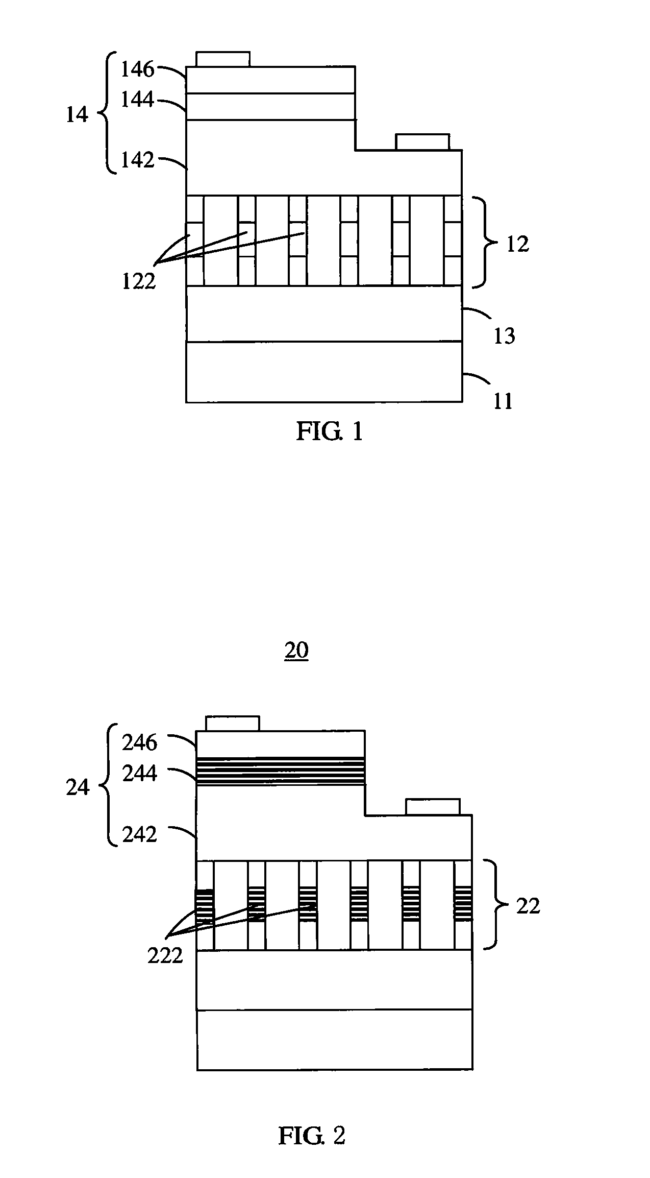
[0027]FIG. 2 is a schematic view of an opto-electronic device in accordance the present application. Referring to FIG. 2, the opto-electronic device 20 is similar in principle to the opto-electronic device 10, and includes a first light-emitting structure 22 and a second light-emitting structure 24. The first light-emitting structure 22 includes a nanorod structure having a first active layer 222. The second light-emitting structure 24 includes an n-type cladding layer 242, a second active layer 244 and a p-type cladding layer 246. However, in the opto-electronic device 20, the first active layer 222 and the second active layer 244 are multiple quantum well structures. Because the multiple quantum well structure has the relatively high photoelectric transformation efficiency, the luminous efficiency of the opto-electronic device 20 can be further improved. In an alternative embodiment, in the opto-electronic device 20, one of the first active layer 222 and the second active layer 24...
third embodiment
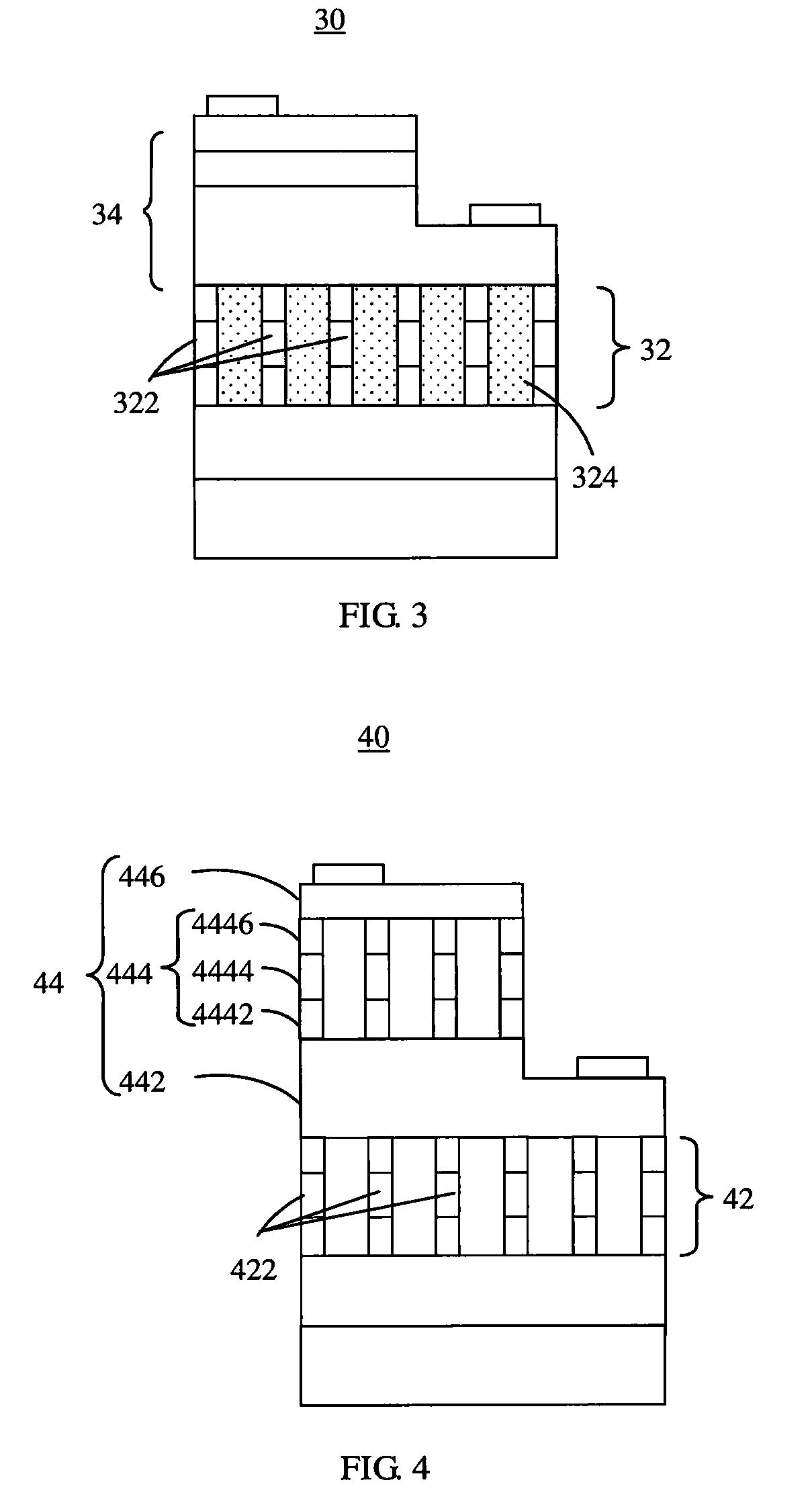
[0028]FIG. 3 is a schematic view of an opto-electronic device in accordance the present application. Referring to FIG. 3, the opto-electronic device 30 is similar in principle to the opto-electronic device 10, and includes a first light-emitting structure 32 and a second light-emitting structure 34. The first light-emitting structure 32 includes a nanorod structure having a plurality of nanorods wherein each of the nanorods includes a first active layer 322. However, in the opto-electronic device 30, the first light-emitting structure 32 further includes a transparent insulation material 324 filled up the space among the nanorods. The transparent insulation material 324 may prevent the nanorods from being affected by the environment. A material of the transparent insulation material 324 can be spin-on glass, silicon dioxide, epoxy resin or other materials having fluorescent powder therein.
PUM
 Abstract
Description
Claims
Application Information
 - Generate Ideas
- Intellectual Property
- Life Sciences
- Materials
- Tech Scout
- Unparalleled Data Quality
- Higher Quality Content
- 60% Fewer Hallucinations
Browse by: Latest US Patents, China's latest patents, Technical Efficacy Thesaurus, Application Domain, Technology Topic, Popular Technical Reports.
© 2025 PatSnap. All rights reserved.Legal|Privacy policy|Modern Slavery Act Transparency Statement|Sitemap|About US| Contact US: help@patsnap.com