Switching converters controlled via sigma delta modulation
a technology of sigma delta modulation and converter, applied in the direction of code conversion, process and machine control, instruments, etc., can solve the problems of pulse-width modulators, and control loops that are typically structured with expensive high-bandwidth and high-accuracy analog-to-digital converters and pulse-width modulators. digitally controlled converters are generally more expensive than their analog versions
- Summary
- Abstract
- Description
- Claims
- Application Information
AI Technical Summary
Problems solved by technology
Method used
Image
Examples
embodiment 20
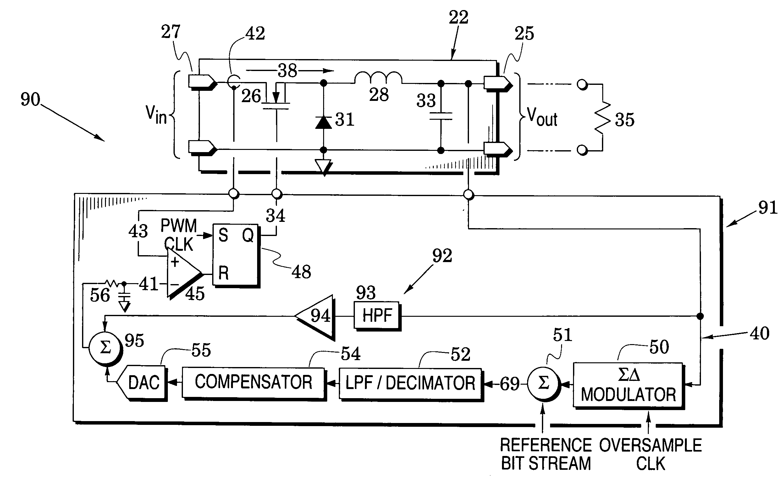
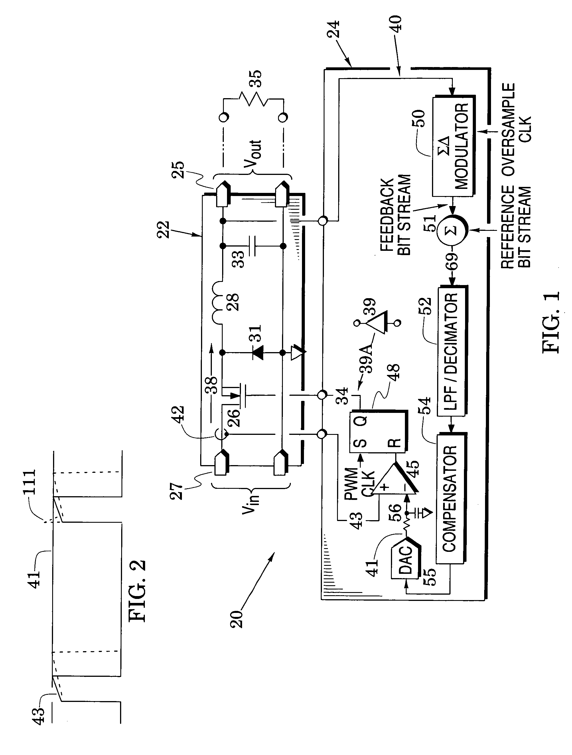
[0017]In particular, FIG. 1 illustrates a switching converter system embodiment 20 that comprises a switching converter 22 in a buck configuration and a controller 24 wherein the converter responds to the controller to thereby generate a controlled output voltage Vout at an output port 25. In an embodiment, the converter 22 includes a switch 26 coupled to an input port 27 and an inductor 28 that is coupled between the transistor and the output port 25. A semiconductor diode 31 is coupled from the junction between the transistor and the inductor to ground and a capacitor 33 is coupled across the output port 25.
[0018]In a converter embodiment, the switch 26 is formed as a metal-oxide semiconductor field-effect transistor (MOSFET) which responds to a pulse-width modulated (PWM) control signal 34 at its control terminal (i.e., its gate). The frequency of the PWM control signal is set by the frequency of a PWM clock provided to a latch of the controller 24. Details of the converter will ...
embodiment 70
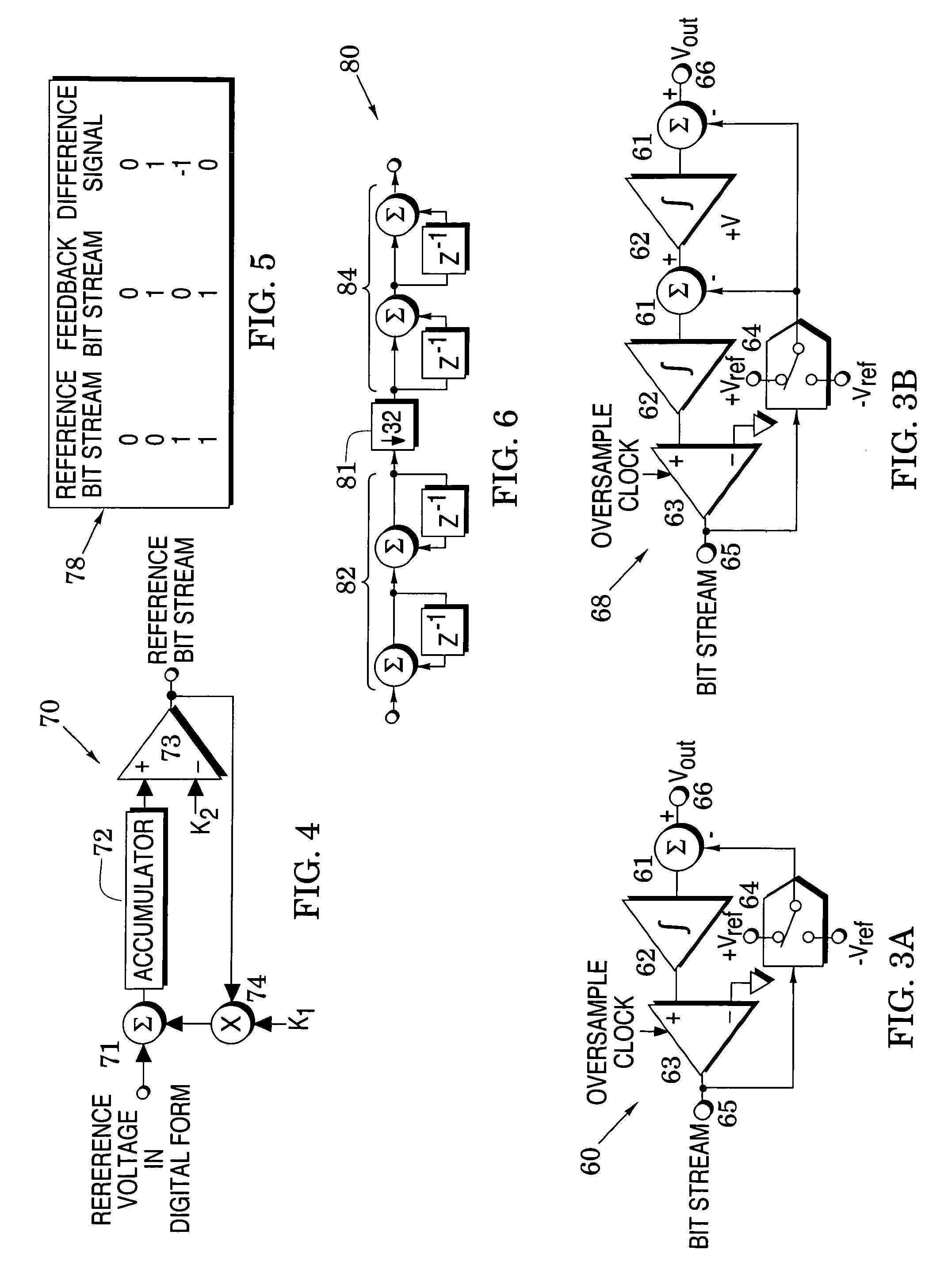
[0034]The reference bit stream in FIG. 1 may be generated with a reference bit stream generator such as the embodiment 70 shown in FIG. 4. This embodiment includes a digital accumulator 72 coupled between an input differencer 71 and a comparator 73. The output of the comparator is fed back to be multiplied in a multiplier 74 by a digital constant K1. The output of the multiplier is provided to the differencer 71 where it is subtracted from the digital representation of the reference voltage. The comparator 73 compares the output of the latch to a second digital constant K2 to produce the reference bit stream.
[0035]In operation, the reference voltage may be expressed with a resolution that is provided by several bits (e.g., 8 bits). The generator 70 operates in response to the oversample clock so that the reference bit stream and feedback bit stream are coincident at the differencer 51 of FIG. 1 to produce the difference signal (69 in FIG. 1). Operation of the differencer is illustra...
embodiment 80
[0036]FIG. 6 illustrates an embodiment 80 of the LPF / Decimator 52 of FIG. 1. This embodiment is a cascaded-integrator-comb (CIC) structure which comprises a downsampling block 81 coupled between an integrator section 82 which operates at the high frequency of the oversample clock and a comb section which operates at the considerably lower frequency of the compensator 54 and DAC 55 in FIG. 1. In this second-order sinc embodiment, the integrator section is formed of two stages of integrators, the comb section is formed of two comb filters and the downsampling block decimates by a factor of 32 (i.e., this embodiment is configured to correspond to an OSR of 32). Register overflow in the integrators can be avoided with sufficient register size (e.g., 11 bits) and by implementing the filter in two's complementary logic to facilitate number wraparound.
PUM
 Abstract
Description
Claims
Application Information


