Efficient Body Contact Field Effect Transistor with Reduced Body Resistance

a field effect transistor and body resistance technology, applied in the field of field effect transistor body resistance reduction, can solve the problems of increasing affecting the efficiency of the body tie, and being difficult to achieve the effect of reducing the body resistance and threshold voltage of the soi transistor

Inactive Publication Date: 2010-04-01
NXP USA INC +1
View PDF1 Cites 29 Cited by
  • Summary
  • Abstract
  • Description
  • Claims
  • Application Information

AI Technical Summary

Problems solved by technology

During device operation, a depleted portion 62 of the extrinsic body tie access region 58 is formed which causes a higher body tie resistance condition, resulting in a degraded body tie efficiency.
And as the size and scaling of semiconductor device technology is reduced, the reduced thickness of the gate dielectric layer 64 results in greater depletion 62 of the body access region 58, which further increases body resistance and threshold voltages for the SOI transistors which can be especially problematic for analog devices.
And with smaller semiconductor devices, aspects of device design and fabrication that previously gave rise to only second-order effects in long-channel devices can no longer be ignored.
For example, the reduced scaling of channel length and gate oxide thickness in a conventional MOS transistor exacerbates problems of polysilicon gate depletion, high gate resistance, high gate tunneling leakage current and dopant (i.e., boron) penetration into the channel region of the device.

Method used


Image

  • Efficient Body Contact Field Effect Transistor with Reduced Body Resistance
  • Efficient Body Contact Field Effect Transistor with Reduced Body Resistance
  • Efficient Body Contact Field Effect Transistor with Reduced Body Resistance

Examples


Embodiment Construction

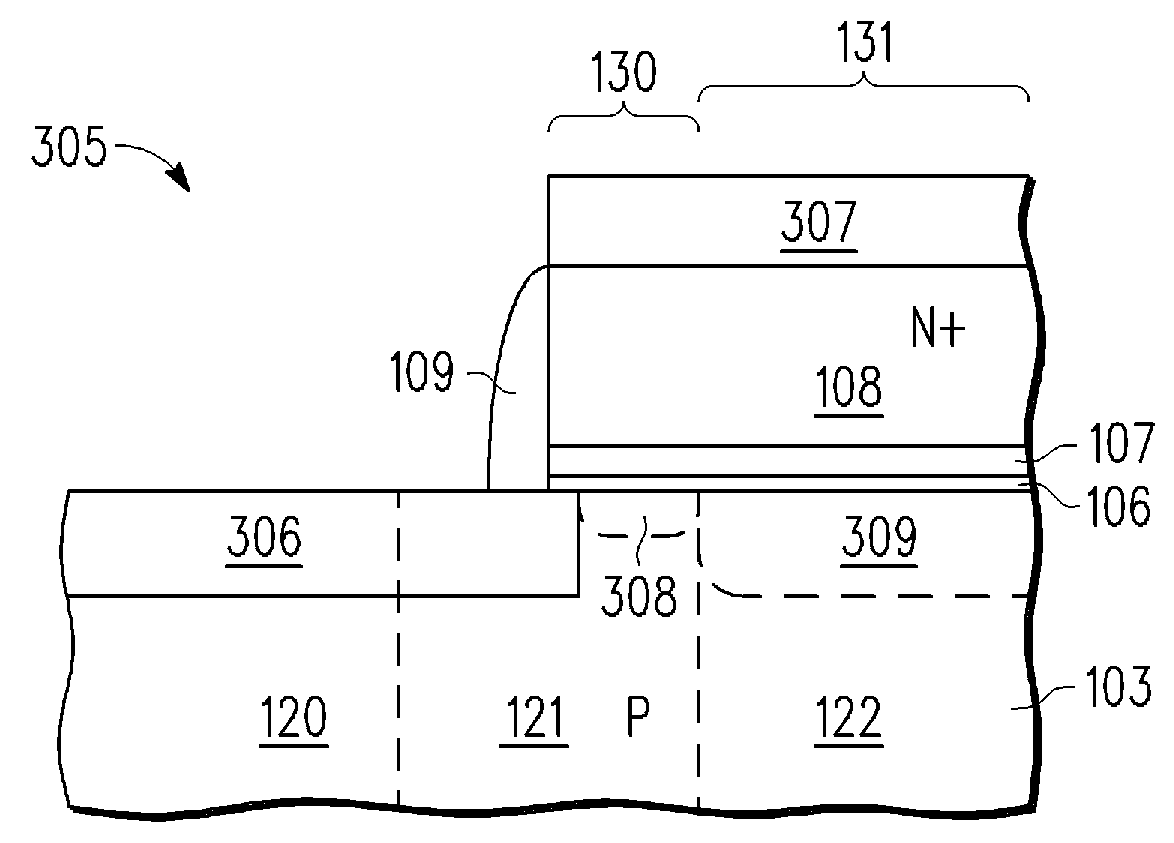
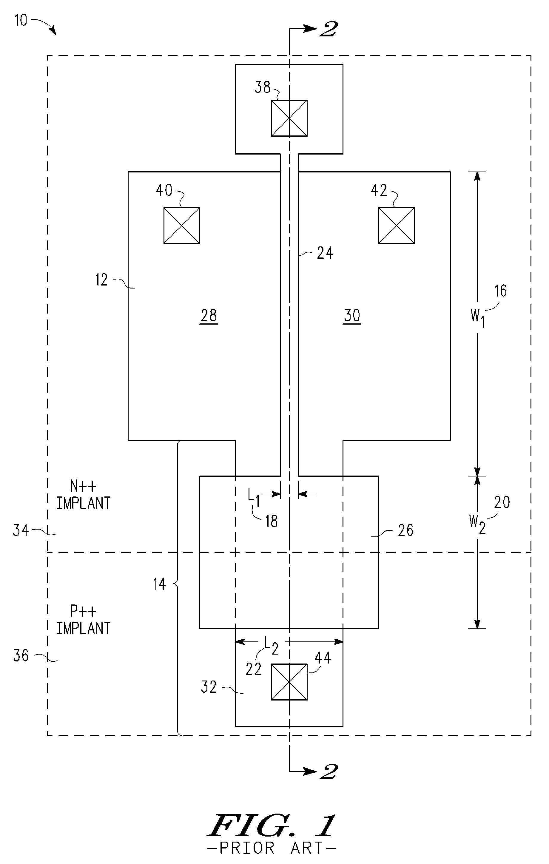
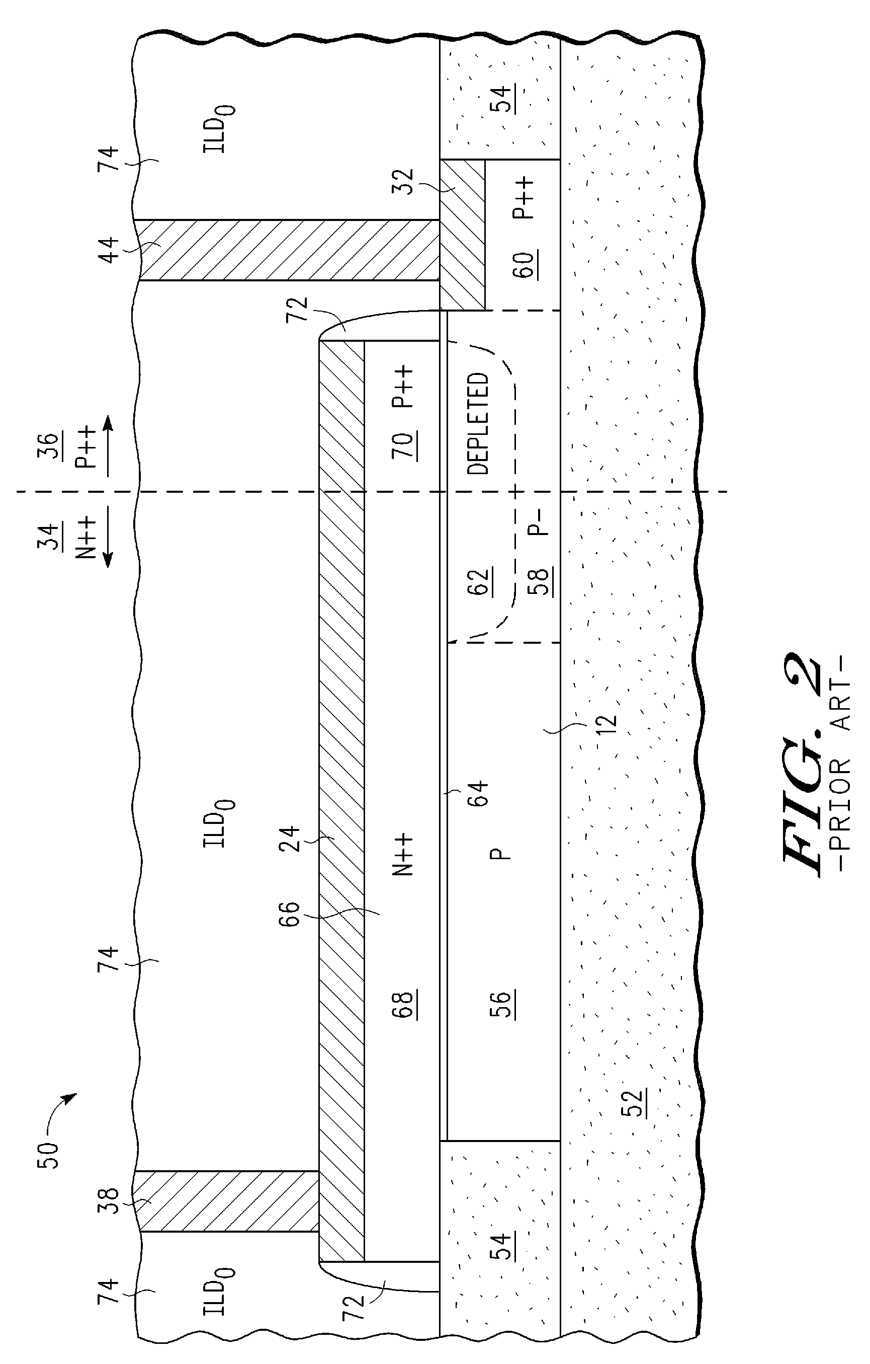
[0023]A semiconductor fabrication process and resulting integrated circuit are described for manufacturing metal gate body-contacted transistor devices, such NMOS or PMOS transistors, over an SOI substrate layer having a lightly doped body region and a body tie access region having reduced body resistance. The method includes forming a metal-based gate electrode and high-k dielectric layer over the SOI substrate to define a source region, a drain region, and a body contact region. In selected embodiments, the method includes selectively counter-doping part of the metal-based gate electrode and body contact region with an implant species having the opposite conductivity type from the remainder of the gate electrode, thereby increasing the voltage threshold Vt in the body access region while lowering the depletion and body contact resistance. In other embodiments, the method includes selectively implanting part of the body contact region with an amorphizing implant species, thereby in...


PUM


Abstract

A method for forming a body contacted SOI transistor includes forming a semiconductor layer (103) having a body contact region (120), a body access region (121), and an active region (122). An SOI transistor is formed in the active region by etching a metal gate structure (107, 108) to have a first portion (130) formed over the active region, and a second portion (131) formed over at least part of the body access region. By implanting ions (203, 301) at a non-perpendicular angle into an implant region (204, 302) in the body access region so as to encroach toward the active region and / or under the second portion of the etched metal gate structure, silicide (306) may be subsequently formed over the body contact region and the implant region, thereby reducing formation of a depletion region (308) in the body access region.

Description

BACKGROUND OF THE INVENTION[0001]1. Field of the Invention[0002]The present invention is directed in general to the field of semiconductor fabrication and integrated circuits. In one aspect, the present invention relates to the formation of a body contact in a field effect transistor.[0003]2. Description of the Related Art[0004]Because of performance limitations associated with conventional field effect transistors formed on bulk semiconductor substrates, semiconductor devices (such as NMOS and PMOS transistors) are increasingly being formed on semiconductor-on-insulator (SOI) substrates in which an active semiconductor layer (in which the transistor devices are formed) is formed over an insulating or dielectric layer (a.k.a., buried oxide layer) which in turn is formed over a bulk semiconductor substrate such that the dielectric layer isolates the active semiconductor layer from the bulk semiconductor substrate. In the active semiconductor layer, SOI transistors are formed by patte...

Claims


Application Information

Patent Timeline
Patent Type & Authority Applications(United States)
IPC IPC(8): H01L21/331
CPCH01L21/26506H01L21/26586H01L29/41758H01L29/7833H01L29/4983H01L29/665H01L29/6659H01L29/4238H01L21/2658
Inventor MIN, BYOUNG W.ZOLLNER, STEFANLIANG, QINGQING
Owner NXP USA INC
Why Eureka
Try Eureka