Tandem nanofilm solar cells joined by wafer bonding

a solar cell and nano-film technology, applied in nanotechnology, pv power plants, semiconductor devices, etc., can solve the problems of reducing yield, reducing efficiency, and increasing costs, so as to optimize the structure of tandem photovoltaic cells, reduce costs, and yield. high

Active Publication Date: 2010-04-08
IBM CORP
View PDF25 Cites 57 Cited by
  • Summary
  • Abstract
  • Description
  • Claims
  • Application Information

AI Technical Summary

Problems solved by technology

A major problem can arise due to the need to prevent diffusion of dopant from any of the layers into adjacent regions; such cross diffusion raises the resistance of the tunnel junctions and lowers efficiency.
In semiconductor fabrication, the simultaneous requirements of tight control of many variables (temperature, time, thicknesses, lattice matching, dopant densities) generally lowers yield and raises costs.
Exfoliation (separation of the desired device volume from the handle substrate) is generally induced by low ion mass ion implantation which causes a weak zone in the material which cracks off upon heating if the ion density is sufficient.

Method used


Image

  • Tandem nanofilm solar cells joined by wafer bonding
  • Tandem nanofilm solar cells joined by wafer bonding
  • Tandem nanofilm solar cells joined by wafer bonding

Examples


Embodiment Construction

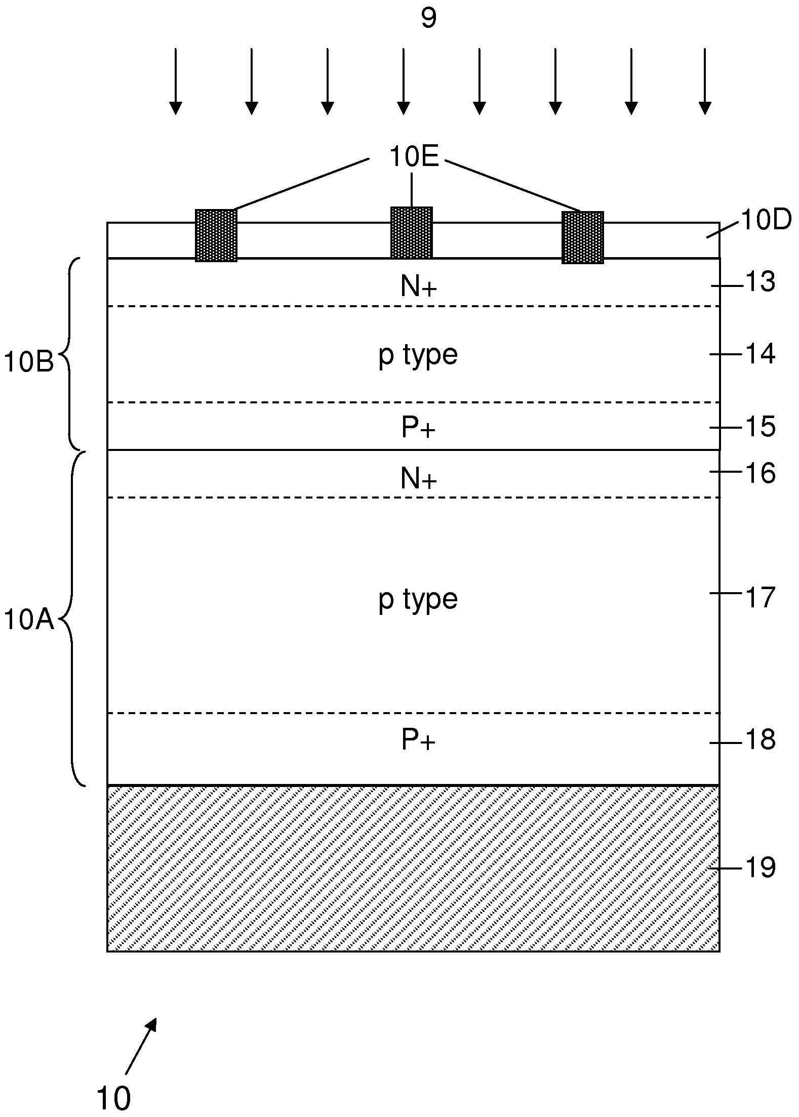
[0029]In FIG. 1, a tandem, multijunction, photovoltaic energy conversion device 10 consisting of two separate, stacked, photovoltaic cells 10A and 10B composed of semiconductor materials and illuminated by radiant energy, e.g. sunlight 9. The lower photovoltaic cell 10A comprises a semiconductor wafer composed of material #1 which contains an N+ doped region 16, a p-type doped region 17, and a P+ doped region 18, is mounted on a substrate 19 using suitable means, such as alloying, adhesive, or bonding. The substrate 19 is composed of a material such as silicon, glass, quartz, silica, alumina, ceramic, metal, graphite, and plastic. The upper photovoltaic cell 10B comprises a semiconductor wafer which is made using a material #2 with a higher bandgap than the material #1 used to make photovoltaic cell 10A, consists of an N+ doped region 13, a P-type doped region 14, and a P+ doped region 15; and the upper photovoltaic cell 10B is mounted to the lower photovoltaic cell 10A using wafer ...


PUM


Abstract

An energy conversion device comprises at least two thin film photovoltaic cells fabricated separately and joined by wafer bonding. The cells are arranged in a hierarchical stack of decreasing order of their energy bandgap from top to bottom. Each of the thin film cells has a thickness in the range from about 0.5 μm to about 10 μm. The photovoltaic cell stack is mounted upon a thick substrate composed of a material selected from silicon, glass, quartz, silica, alumina, ceramic, metal, graphite, and plastic. Each of the interfaces between the cells comprises a structure selected from a tunnel junction, a heterojunction, a transparent conducting oxide, and an alloying metal grid; and the top surface and / or the lower surface of the energy conversion device may contain light-trapping means.

Description

CROSS-REFERENCE TO RELATED APPLICATIONS[0001]This application contains subject matter which is related to the subject matter of the following commonly assigned copending applications, including U.S. patent application Ser. No. 12 / 242,962 filed on 1 Oct. 2008 entitled “Optical Tandem Photovoltaic Cell Panels” (Attorney Docket No. YOR920070443US1); and U.S. patent application Ser. No. 12 / 243,995 filed on 2 Oct. 2008 entitled “Quantum Well Gap / Si Tandem Photovoltaic Cells” (Attorney Docket No. YOR920070447US1.) Each of the above listed patent applications is hereby incorporated herein by reference in its entirety.BACKGROUNDDefinitions[0002]Electromagnetic Radiation to Electric Energy Conversion Device (EREECD): A device that reacts with electromagnetic (optical) radiation to produce electrical energy[0003]Optical Radiation to Electric Energy Conversion Device (OREECD): A device that reacts with optical electromagnetic radiation to produce electrical energy. Such a device could be a rad...

Claims


Application Information

Patent Timeline
Patent Type & Authority Applications(United States)
IPC IPC(8): H01L31/042
CPCB82Y20/00H01L31/0236H01L31/035236H01L31/0687H01L31/0693H01L31/0547Y02E10/544H01L31/053H01L31/0725H01L31/18Y02E10/52H01L31/022433H01L31/02366H01L31/1884
Inventor HOVEL, HAROLD J.
Owner IBM CORP
Why Eureka
Try Eureka