Light coupler between an optical fibre and a waveguide made on an soi substrate

a technology of which is applied in the field of light couplers between optical fibers and waveguides made on soi substrates, can solve the problems of incompatibility of sensitivity, significant, and loss of 2 db, and achieve linear decrease of the width of the rib of the waveguide forming the injector, and invariant width

Active Publication Date: 2010-04-08
COMMISSARIAT A LENERGIE ATOMIQUE ET AUX ENERGIES ALTERNATIVES
View PDF7 Cites 84 Cited by
  • Summary
  • Abstract
  • Description
  • Claims
  • Application Information

AI Technical Summary

Benefits of technology

[0014]The rib of the waveguide forming the injector may have invariant width. According to another alternative embodiment, the rib of the waveguide forming the injector has an adiabatic shape, its width decreasing from its face for receiving the end of the optical fiber. According to an alternative embodiment, the width of the rib of the waveguide forming the injector decreases linearly.
[0015]According to an alternative embodiment, the width of the nanotip forming the collector decreases from its second end in a way selected from a linear decrease, a polynomial decrease and an exponential decrease.

Problems solved by technology

Another difficulty relates to polarisation of light: the optical signal circulating in fiber networks does not have any definite polarisation: it is a random quantity which continuously changes over time.
On reception, this sensitivity is incompatible with direct connection of the circuit to the network of optical fibers in which the state of polarisation is both unknown and unstable.
The major drawback of this approach is that the obtained device only operates for TE (transverse electric) polarisation and that the losses are quite high (typically −2 db).
Another difficulty, also significant, relates to the encapsulation and reliability of the proposed structure.
Further, the polymer does not retain its properties over time and under a strong light flux.

Method used


Image

  • Light coupler between an optical fibre and a waveguide made on an soi substrate
  • Light coupler between an optical fibre and a waveguide made on an soi substrate
  • Light coupler between an optical fibre and a waveguide made on an soi substrate

Examples


Embodiment Construction

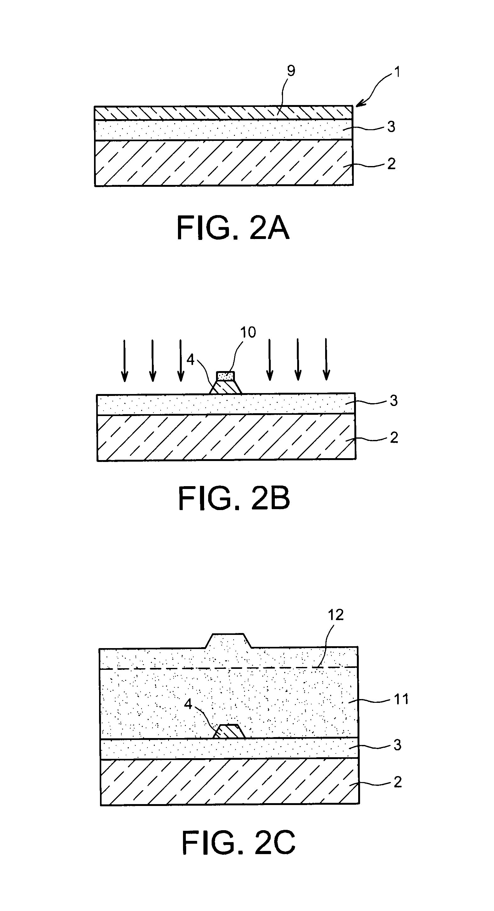
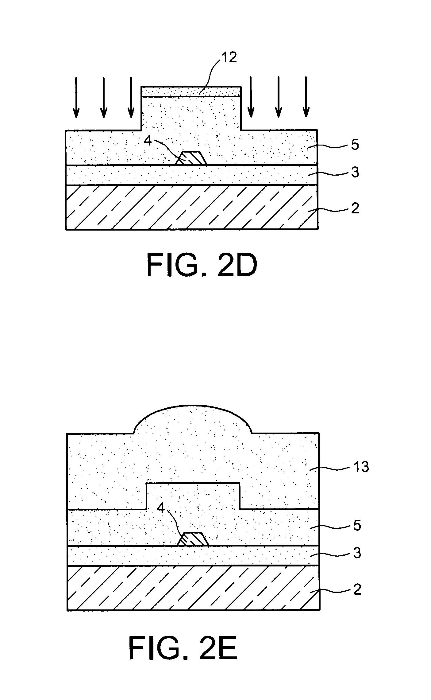
[0032]The injector has a very specific shape. The latter has a geometry of the rib guide type. The collector is always positioned downstream from the injector. Advantageously, the nanotip has an initial width of less than the tenth of the minimum operating wavelength in order to avoid problems related to diffraction of the optical mode. The coupling of the injected mode is accomplished gradually as the width of the collector increases until it attains that of the waveguide.

[0033]In the following of the description, embodiments implemented on an SOI substrate will be described.

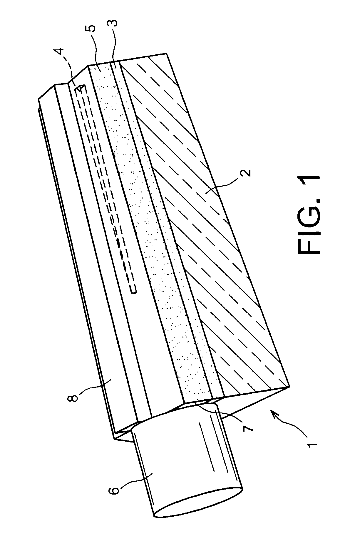
[0034]FIG. 1 is a perspective, partly sectional view of a light coupler according to the present invention. The coupler is made on an SOI substrate 1. The substrate 1 comprises a support 2, for example in silicon, successively supporting a silicon oxide layer 3, called a buried oxide layer or BOX and with an optical index of 1.45, and a thin silicon layer.

[0035]The waveguide is made on the SOI substrate 1. The ...


PUM

PropertyMeasurementUnit
thicknessaaaaaaaaaa
widthaaaaaaaaaa
widthaaaaaaaaaa

Abstract

A light coupler between an optical fiber (6) and a waveguide is made on a semiconductor-on-insulator substrate (1), this substrate (1) comprising a thin layer of semiconducting material in which the waveguide is made. The coupler comprises a light injector (5) and an adiabatic collector (4) made up with an inverted nanotip formed from the thin layer of semiconducting material. The injector (5) is formed on the insulator (3) and has a face (7) for receiving an end of the optical fiber (6). The adiabatic collector (4) has a cross-section which increases from a first end located on the side of said end of the optical fiber (6) right up to a second end which is connected to the waveguide, the injector (5) covering the adiabatic collector (4) and having a rib waveguide shape.

Description

TECHNICAL FIELD[0001]The invention relates to a light coupler between an optical fiber and a waveguide made on an SOI substrate. Such a light coupler finds applications in the field of optoelectronics and notably for nanophotonic circuits.STATE OF THE PRIOR ART[0002]Optoelectronic components made from microstructured or nanostructured planar optical guides allow the implementation of functions which are specific to them (resonator, wavelength multiplexer / demultiplexer, coupler, . . . ) and also with them it is possible to obtain effective coupling between an optical fiber for communication with external circuits.[0003]Optoelectronic coupling components are notably involved in data transmission networks via optical fiber and in integrated (intra-chip and inter-chip) photonic circuits. Such a component may be considered as a basis brick of more complex devices.[0004]With technologies of planar optical guides, it is possible to integrate in a compact way and on a same chip, complex fun...

Claims


Application Information

Patent Timeline
Patent Type & Authority Applications(United States)
IPC IPC(8): G02B6/30G02B6/26C23F1/00
CPCG02B6/305G02B6/1228Y10S977/721Y10S977/932
Inventor BEN BAKIR, BADHISEFEDELI, JEAN-MARC
Owner COMMISSARIAT A LENERGIE ATOMIQUE ET AUX ENERGIES ALTERNATIVES
Why Eureka
Try Eureka