Semiconductor device and RFID tag chip

a technology of rfid tag and semiconductor device, which is applied in the field of constant voltage circuits, can solve the problems of mounting cost and test cost, difficult to trim a plurality of chips at the same time, and cannot be only focused on reducing so as to achieve low cost, reduce the manufacturing cost of the circuit, and reduce the effect of mounting cos

Inactive Publication Date: 2010-04-15
RENESAS ELECTRONICS CORP
View PDF3 Cites 14 Cited by
  • Summary
  • Abstract
  • Description
  • Claims
  • Application Information

AI Technical Summary

Benefits of technology

[0011]However, attention cannot be paid only to reduction in manufacturing cost of the circuits. When an RFID tag chip is provided as a product, mounting costs and test costs also exist. To supply an RFID tag chip at low cost, it is important to reduce also those costs.

Problems solved by technology

However, attention cannot be paid only to reduction in manufacturing cost of the circuits.
When an RFID tag chip is provided as a product, mounting costs and test costs also exist.
As for trimming, it is difficult to trim a plurality of chips at the same time.
The BGR circuit, however, has another problem.
A problem occurs particularly at the startup of Vdd.

Method used


Image

  • Semiconductor device and RFID tag chip
  • Semiconductor device and RFID tag chip
  • Semiconductor device and RFID tag chip

Examples


first embodiment

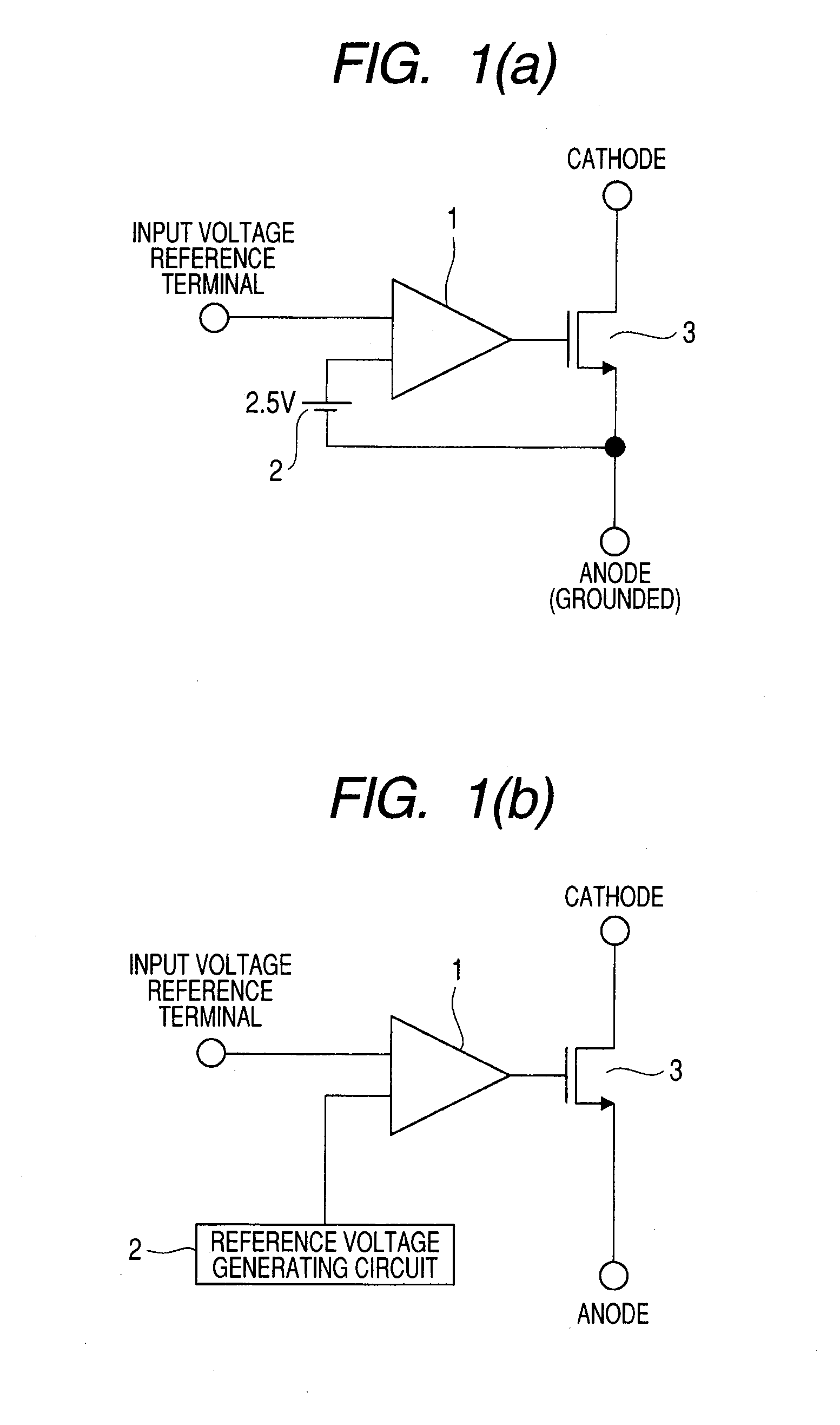
[0046]FIGS. 1A and 1B are circuit diagrams showing the configuration of a shunt regulator as a kind of a constant voltage power supply circuit. FIG. 1A shows the configuration of a constant voltage power source circuit used for a stationary device having a stable power source supplied from the outside, and FIG. 1B illustrates the configuration of a constant voltage power source circuit of a device that generates a power source voltage from an electric wave or the like, such as a noncontact RFID tag chip as an object of the present invention.

[0047]A shunt regulator of FIG. 1A has an amplifier 1 functioning as a comparator, a MOS-FET 3 in which gate voltage changes according to an output of the amplifier 1, and a reference voltage source 2′ as a reference in comparison in the amplifier 1. In the case where an apparatus itself does not have a power supply like an RFID tag chip, it is unpreferable to provide a reference voltage source. Therefore, it is requested to generate a reference ...

second embodiment

[0150]A second embodiment of the present invention will now be described with reference to the drawings.

[0151]The Vth difference reference circuit used in the first embodiment does not have to generate a high-precision reference voltage as long as it can realize prompt rise.

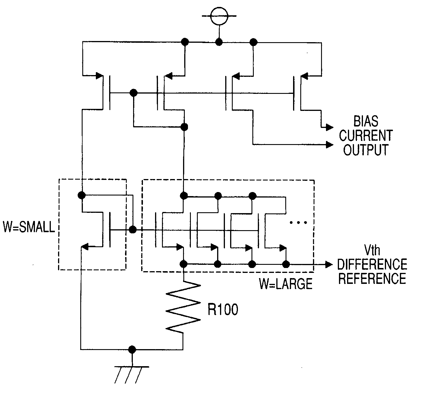
[0152]FIG. 19 is a diagram showing a circuit for generating constant current called a Widlar current source used in a second embodiment of the invention. The Widlar current source is a circuit generally used in the field of LSIs.

[0153]The Widlar current source is a circuit for passing the same current to a MOS-FET having a large gate width W and a MOS-FET having a small width W (in the diagram, expressed as parallel MOS-FETs) by a current mirror circuit, and sending the Vgs difference of the MOS-FETs and a resistance value of R100 as a feedback so that the current becomes constant regardless of the power supply voltage.

[0154]Since the Vgs difference of the Widlar current source is constant regardless of the power...


PUM


Abstract

The present invention provides a reference power supply circuit which does not require trimming and prevents occurrence of deadlock of a band gap reference circuit. An RFID tag chip related to the present invention has a reference power supply including a switch for switching between a band gap reference circuit and a Vth difference reference circuit. A reference potential in band gap reference of the band gap reference circuit and an output of the Vth difference reference circuit are compared by a comparator, and a transistor operating as a switch is controlled, thereby making the reference potential in band gap reference rise, hastening startup of the band gap reference circuit, and preventing occurrence of deadlock in the band gap reference circuit.

Description

CROSS-REFERENCE TO RELATED APPLICATIONS[0001]The disclosure of Japanese Patent Application No. 2008-263596 filed on Oct. 10, 2008 including the specification, drawings and abstract is incorporated herein by reference in its entirety.BACKGROUND OF THE INVENTION[0002]The present invention relates to a constant voltage circuit for use in an RFID tag chip or the like and, more particularly, to a process of starting power at the time of start-up.[0003]In recent years, the number of chips operating on power received from electric waves is increasing. One of such chips is an RFID tag chip (hereinbelow, called RFID tag chip). One of uses of the RFID tag chip is to identify a person or object by radio.[0004]Basically, unique numbers are assigned to all of RFID tag chips. A reader / writer can read a unique number by radio communication. Since the operation of associating numbers and chips is performed on the reader / writer side, an RFID tag chip itself does not have a complicated function. Acco...

Claims


Application Information

Patent Timeline
Patent Type & Authority Applications(United States)
IPC IPC(8): G06K19/06H01L23/52
CPCG06K19/0701G06K19/0723H03K3/011H03K3/0315H01L2924/0002H03K17/693H01L2924/00
Inventor OKUDA, YUICHI
Owner RENESAS ELECTRONICS CORP
Why Eureka
Try Eureka