Soi substrate and method for producing the same, solid-state image pickup device and method for producing the same, and image pickup apparatus

Inactive Publication Date: 2010-04-15
SONY CORP
View PDF78 Cites 48 Cited by
  • Summary
  • Abstract
  • Description
  • Claims
  • Application Information

AI Technical Summary

Benefits of technology

[0042]In the image pickup apparatus according to an embodiment of the present invention, the use of the solid-state image pickup device according to an embodiment of the present invention reduces the degree of metal contamination in the silicon layer where the photoelectric conversion unit is formed.
[0043]In the image pickup app

Problems solved by technology

A problem to be solved is that in the case where a contaminant such as a metal impurity enters a single-crystal silicon layer of a SOI substrate from the side of its surface, the contaminant is accumulated in the single-crystal silicon layer because the metal

Method used


Image

  • Soi substrate and method for producing the same, solid-state image pickup device and method for producing the same, and image pickup apparatus
  • Soi substrate and method for producing the same, solid-state image pickup device and method for producing the same, and image pickup apparatus
  • Soi substrate and method for producing the same, solid-state image pickup device and method for producing the same, and image pickup apparatus

Examples


Example

1. First Embodiment

First Example of Structure of SOI Substrate

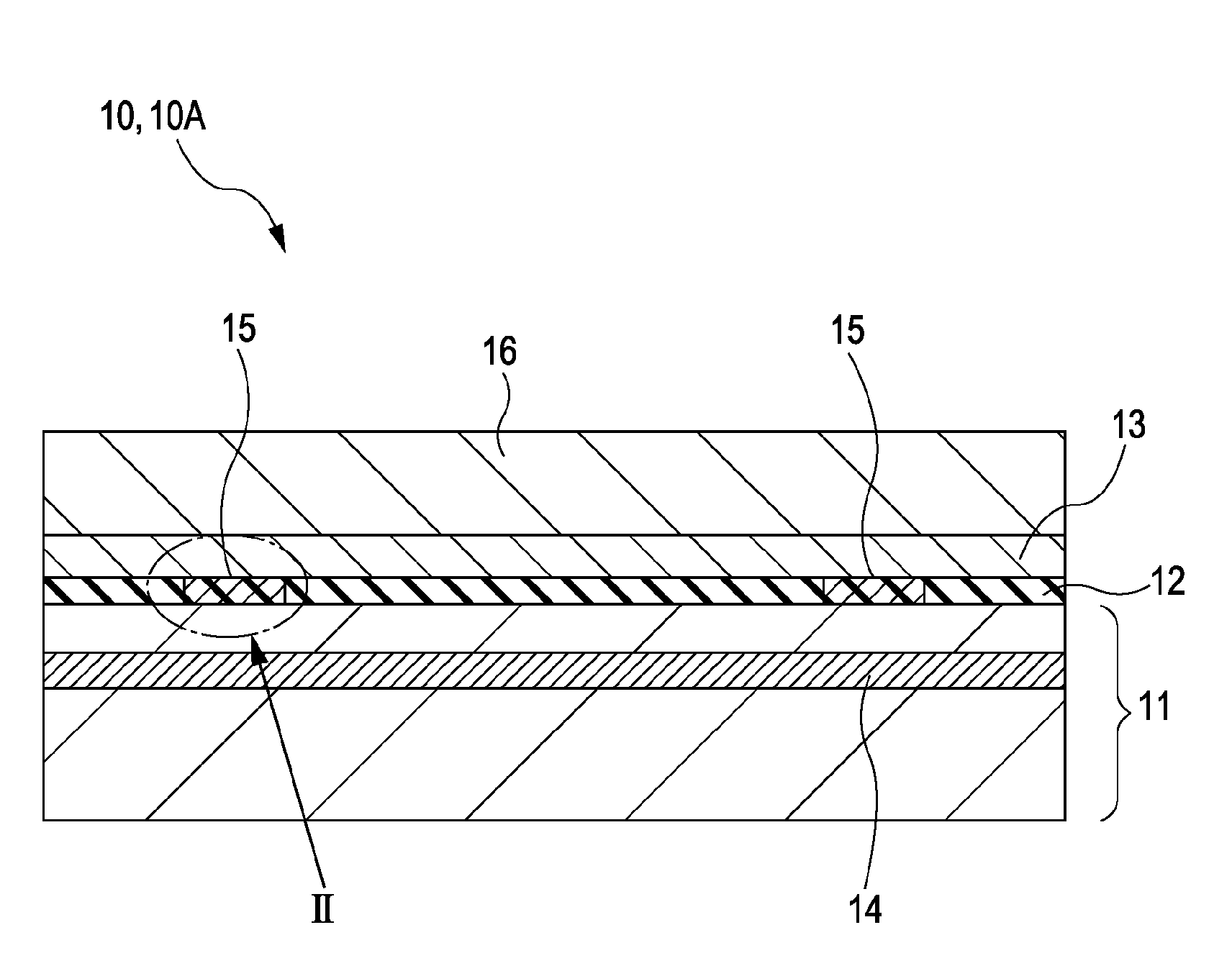
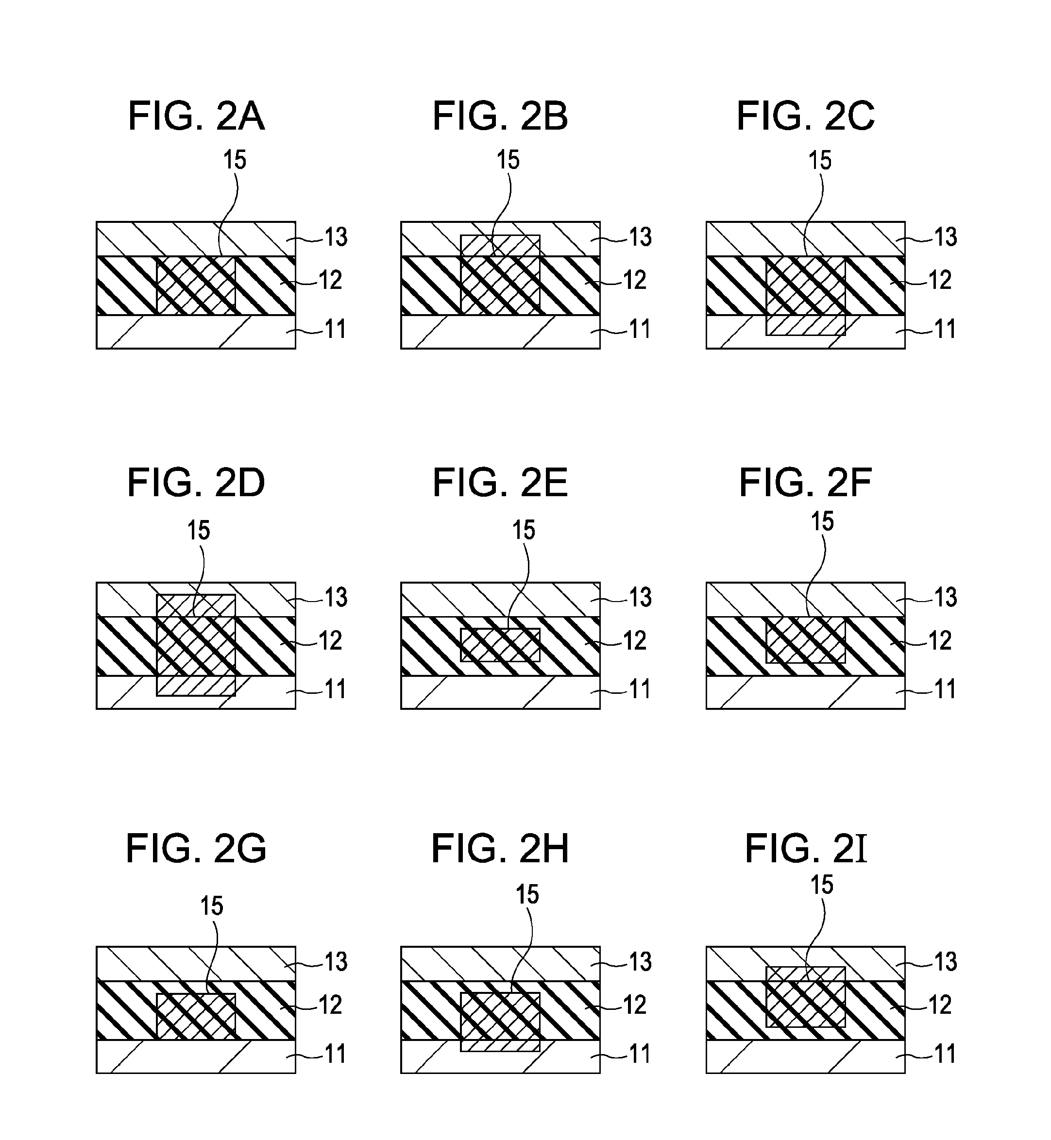
[0076]A first example of the structure of a SOI substrate according to a first embodiment of the present invention will be described with reference to FIG. 1 which is a schematic cross-sectional view.

[0077]As shown in FIG. 1, a silicon oxide layer 12 (for example, also referred to as a “box layer”) is arranged on a silicon substrate 11. As the silicon substrate 11, for example, a single-crystal silicon substrate is used. The silicon oxide layer 12 is overlaid with a silicon layer 13. The silicon layer 13 is formed by bonding the silicon oxide layer 12 to the single-crystal silicon substrate and reducing the thickness of the single-crystal silicon substrate.

[0078]The silicon substrate 11 includes a gettering layer 14. The gettering layer 14 is formed of a region into which one element selected from carbon (C), oxygen (O), argon (Ar), silicon (Si), helium (He), phosphorus (P), arsenic (As), antimony (Sb), and boron (B) is i...

Example

2. Second Embodiment

First Example of Method for Producing SOI Substrate

[0162]A first example of a method for producing a SOI substrate according to a second embodiment of the present invention will be described below with reference to figures showing cross-sectional views illustrating the steps in the method.

[0163]First, a method for producing a SOI substrate with a gettering layer by the Smart Cut process will be described below with reference to figures showing cross-sectional views illustrating the steps in the method.

[0164]As shown in FIG. 7A, a first substrate 21 is prepared. As the first substrate 21, for example, a silicon substrate is used.

[0165]As shown in FIG. 7B, the silicon oxide layer 12 is formed on surfaces of the first substrate 21 by thermal oxidation so as to have a thickness of, for example, 500 nm.

[0166]As shown in FIG. 7C, a split layer 17 is formed in the first substrate 21 by ion implantation. For example, the split layer 17 is formed in such a manner that a p...

Example

3. Third Embodiment

Example of Structure of Solid-State Image Pickup Device

[0416]An exemplary structure of a solid-state image pickup device according to a third embodiment will be described with reference to FIG. 23 showing a schematic cross-sectional view. FIG. 23 shows an example of a solid-state image pickup device of a stacked whole-area-open-type CMOS image sensor.

[0417]As shown in FIG. 23, the silicon layer 13 and the epitaxially grown silicon layer 16 formed of a silicon layer grown on the silicon layer 13 of the SOI substrate are used as an active layer. Photoelectric conversion units 61, pixel transistors 63, and a peripheral circuit (not shown) are arranged in the epitaxially grown silicon layer 16.

[0418]In view of forming the photoelectric conversion units 61, for example, the epitaxially grown silicon layer 16 with a thickness of about 8 μm is adequate to form the photoelectric conversion units 61 sensitive to long wavelengths of near-infrared and infrared region. For ex...


PUM


Abstract

A SOI substrate includes a silicon substrate, a silicon oxide layer arranged on the silicon substrate, a silicon layer arranged on the silicon oxide layer, a gettering layer arranged in the silicon substrate, and a damaged layer formed of an impurity-doped region arranged in the silicon oxide layer.

Description

BACKGROUND OF THE INVENTION[0001]1. Field of the Invention[0002]The present invention relates to a silicon-on-insulator (SOI) substrate, a method for producing the substrate, a solid-state image pickup device, a method for producing the device, and an image pickup apparatus.[0003]2. Description of the Related Art[0004]Silicon on insulator (SOI) substrates have recently been receiving attention in the field of image sensors as well as high-density CMOS elements and high-withstand-voltage elements because a significant increase in sensitivity should be obtained. For example, SOI substrates are used in whole-area-open-type CMOS image sensors. It is desired to have a higher gettering ability.[0005]Specifically, a SOI substrate has a three-layer structure in which a single-crystal silicon layer used as a device formation region is arranged on a support substrate with a buried insulating film such as a silicon oxide (SiO2) film. In some cases, an epitaxial grown layer is arranged on the s...

Claims


Application Information

Patent Timeline
IPC IPC(8): H01L31/0232H01L29/30H01L21/322H01L21/762H01L31/18H01L21/02H01L21/20H01L21/265H01L27/12H01L27/146
CPCH01L21/26506H01L21/3226H01L21/76254H01L27/1464H01L27/14621H01L27/14683H01L27/14601H01L21/2658H01L21/26566H01L21/20H01L27/146
Inventor TAKIZAWA, RITSUO
Owner SONY CORP
Why Eureka
Try Eureka