High efficiency multijunction ii-vi photovoltaic solar cells

a photovoltaic solar cell, multi-junction technology, applied in photovoltaics, electrical equipment, semiconductor devices, etc., can solve the problems of large heat generation from excess energy of hot carriers, low output current, and relatively low photovoltage, so as to prevent damage

Active Publication Date: 2010-04-22
EPIR TECH INC
View PDF51 Cites 132 Cited by
  • Summary
  • Abstract
  • Description
  • Claims
  • Application Information

AI Technical Summary

Benefits of technology

[0033]As in the other embodiments, it is preferred that degeneratively alloyed tunnel junctions be formed between adjacent ones of the subcells, and that the subcell stack be capped with an antireflective coating with a ba

Problems solved by technology

One disadvantage of such a photovoltaic solar cell is that the photovoltage is relatively low due to the small energy gap of the absorber.
Another disadvantage of a small energy gap photovoltaic solar cell is that hot carriers are generated by the incident photons with energy much greater than the energy gap, and hence the excess energy of the hot carriers produces a large amount of heat in the thermalization process unless the higher energy photons are absorbed before reaching the narrow-gap material.
The disadvantage of such a photovoltaic solar cell is that a large number of incident photons have energies below the energy gap of the base layer semiconductor and hence are not absorbed, so that the output current is relatively low.
But, in practice, the base layer energy gaps of a multijunction solar cell only cover a portion of the entire solar spectrum.
First, according to the commonly accepted wisdom, epitaxial growth is best performed on lattice matched substrates and on lattice matched epilayers, and it is very difficult to lattice match substrate

Method used


Image

  • High efficiency multijunction ii-vi photovoltaic solar cells
  • High efficiency multijunction ii-vi photovoltaic solar cells
  • High efficiency multijunction ii-vi photovoltaic solar cells

Examples


first embodiment

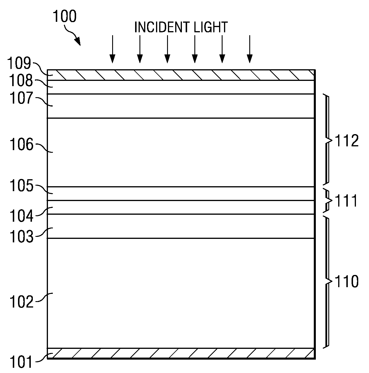
[0047]In this first embodiment of the invention, the material system that is used for the first tunnel junction 111 is not limited to ZnTe semiconductors, but can be made from other relatively high energy gap materials such as CdS (EgCdS≈2.46 eV), ZnSe (EgZnSe≈2.72 eV), MgTe (EgMgTe≈3.40 eV), ZnS (EgZnS≈3.73 eV), CdZnTe (EgCdZnTe≈1.8 to 2.26 eV), CdMgTe (EgCdMgTe≈1.8 to 3.3 eV), CdMnTe (EgCdMnTe≈1.8 to 2.92 eV), and ZnMnSe (EgZnMnSe≈2.8 to 3.30 eV) compound semiconductors. The energy gaps (EgTJ1B and EgTJ1E) of the first tunnel junction 111 must be greater than those of the first emitter 103 (Eg1E) of the first subcell 110 and the second base 106 (Eg2B) of the second subcell 112. In addition, the (p++) and (n++) tunnel junction with homo-interface (homojunction) can be replaced by a tunnel junction with a hetero-interface (heterojunction) that comprises thin layers semiconductor material having different energy gaps. The first tunnel junction is designed in such a way that the tunne...

second embodiment

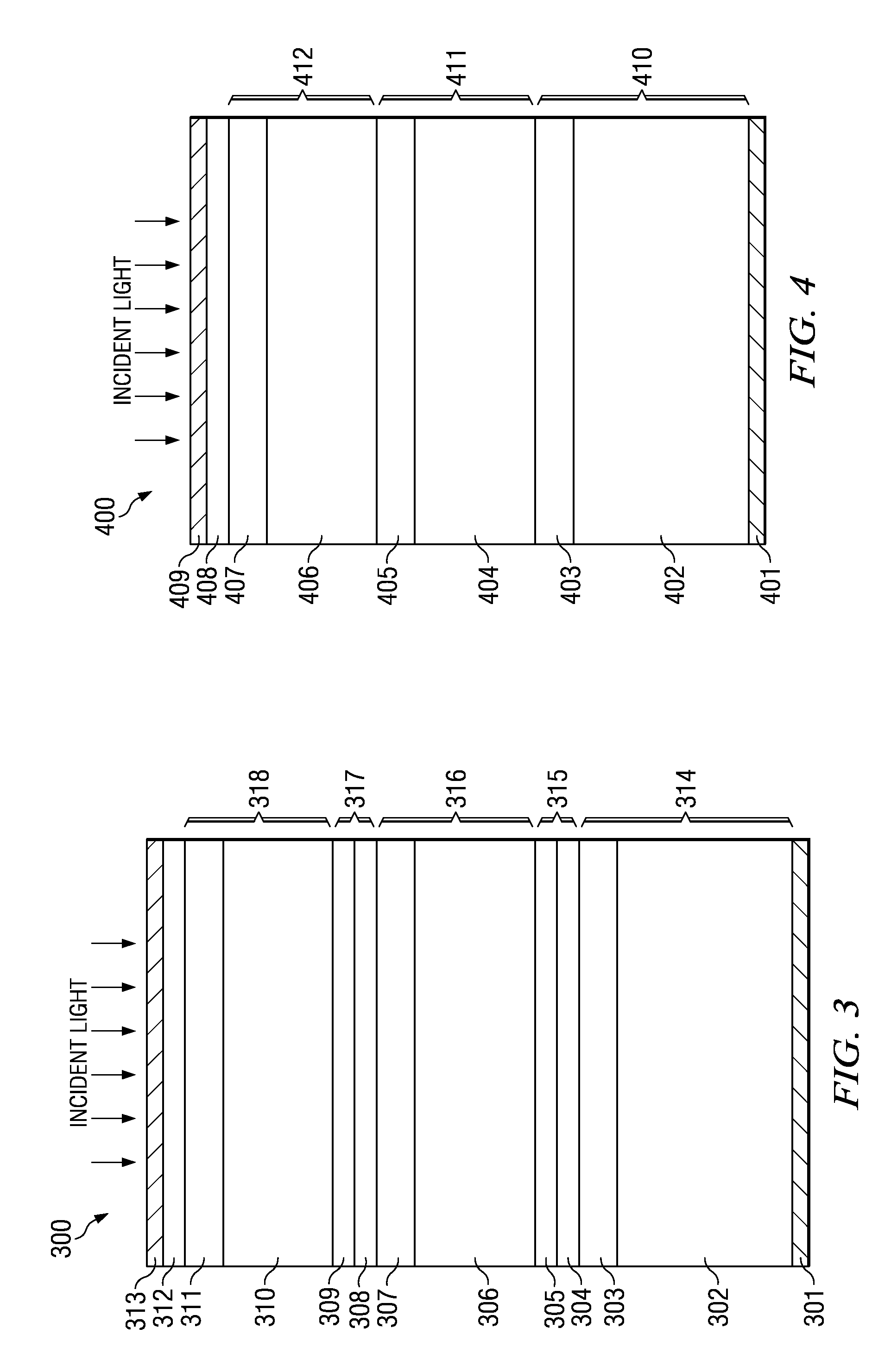
[0059]A three-subcell photovoltaic solar cell is schematically illustrated in FIG. 3. This second embodiment encompasses the embodiment shown in FIG. 1 and described above with an additional subcell and preferably a second tunnel junction. The preferred three-subcell photovoltaic solar cell 300 ((n+)ZnO / (n+)Cd1-xZnxTe / (p−)Cd1-xZnxTe / (p++)ZnTe / (n++)ZnTe / (n+)CdTe / (p−)CdTe / (p++)ZnTe / (n++)ZnTe / (n+)Si / (p−)Si where the mole fraction x 0.31) includes a first subcell 314, a second subcell 316 formed over the subcell 314, a third subcell 318 formed over the second subcell 316, a first tunnel junction 315 interposed between subcells 314 and 316, a second tunnel junction 317 disposed between subcells 316 and 318, an antireflection coating 312, formed above the topmost subcell 318 to provide protection against photons with energies higher than the bandgaps of third subcell 318, a front contact 313, and a back contact 301. The third subcell 314, which is disposed immediately adjacent to the seco...

fourth embodiment

[0101]In another variation of the present invention, the (p−) and (n) semiconductor layers of cell 800 are reversed.

[0102]The invention discloses, for the first time, several monolithic multi-subcell photovoltaic solar cells having no Group III-V semiconductors and having ideal overall series efficiencies of at least 45% under concentrated sunlight of approximately 500 suns. These ideal energy conversion efficiencies have not been reported before for solar cells composed of any monatomic or compound semiconductor family or combination of such families or material systems (Groups IV, III-V, or II-VI).

[0103]In summary, several monolithic multi-junction or -subcell photovoltaic solar cells have been described which are fabricated of a combination of Group IV and Group II-VI materials, preferably on silicon substrates. Species, alloys, and thicknesses of successively grown layers can be selected to create solar cells having more than fifty percent ideal overall energy conversion efficie...


PUM


Abstract

A Group II-VI photovoltaic solar cell comprising at least two and as many as five subcells stacked upon one another. Each subcell has an emitter layer and a base layer, with the base of the first subcell being made of silicon, germanium, or silicon-germanium. The remaining subcells are stacked on top of the first subcell and are ordered such that the band gap gets progressively smaller with each successive subcell. Moreover, the thicknesses of each subcell are optimized so that the current from each subcell is substantially equal to the other subcells in the stack. Examples of suitable Group II-VI semiconductors include CdTe, CdSe, CdSeTe, CdZnTe, CdMgTe, and CdHgTe.

Description

RELATED APPLICATIONS[0001]This application is a continuation in part of U.S. patent application Ser. No. 12 / 256,247 filed 22 Oct. 2008, the specification of which is fully incorporated by reference herein.BACKGROUND OF THE INVENTION[0002]Photovoltaic solar cells have many applications. Solar cell systems may be connected to an electric utility grid or be used independently. Applications include water heating, residential electric power, electric power for buildings, generation of power for electric utilities, applications in space, military applications, electric power for automobiles, airplanes, etc., and low-power specialty applications. Solar cells may be used in rooftop systems, in sheets rolled out on large flat areas in the desert or elsewhere, on systems that track the motion of the sun to gain the maximum incident solar power, with or without lenses and / or curved reflectors to concentrate the sun's light on small cells, in folding arrays on satellites and spacecraft, on the ...

Claims


Application Information

Patent Timeline
IPC IPC(8): H01L31/042H01L31/00
CPCY02E10/544H01L31/0687
Inventor SIVANANTHAN, SIVALINGAMLAU, WAYNE H.GREIN, CHRISTOPHGARLAND, JAMES W.
Owner EPIR TECH INC
Why Eureka
Try Eureka