Light-emitting device

a light-emitting device and light-emitting technology, which is applied in the direction of solid-state devices, lasers, semiconductor lasers, etc., can solve the problems of affecting the brightness of the display, the irregularities of the polarized light, and the increase of the loss of the polarization plate on the incidence side, so as to achieve excellent end faces and maximize energy utilization. , the effect of efficient generation

Active Publication Date: 2010-04-22
ROHM CO LTD
View PDF8 Cites 307 Cited by
  • Summary
  • Abstract
  • Description
  • Claims
  • Application Information

AI Technical Summary

Benefits of technology

[0028]Preferably, the electrode is in the form of stripes along the c-axis direction. According to the structure, light propagated in the c-axis direction can be extracted. Further, a spontaneous emission component contributing to laser oscillation can be efficiently generated in a case of constituting a semiconductor laser diode, for example.
[0029]The light-emitting device may be a laser diode having a pair of end faces parallel to a c-plane. According to the structure, a light output in the c-axis direction is high, whereby a light emitting element contributing to oscillation can be efficiently utilized.
[0030]Preferably, the end faces are defined by cleavage planes. According to the structure, an individual device can be prepared by cleavage and excellent end faces are obtained, whereby a laser diode excellent in mass productivity can be implemented. Further, c-planes are symmetry planes, whereby the same are excellent in cleavability, a...

Problems solved by technology

When a GaN semiconductor layer having a major surface defined by a nonpolar plane or a semipolar plane is employed to emit polarized light, however, the polarized light is disturbed by irregularities of a rough surface if a surface of the GaN semiconductor layer on a light extraction side or a surface of an electrode on the light extraction side is the rough surface.
When...

Method used


Image

  • Light-emitting device
  • Light-emitting device
  • Light-emitting device

Examples


second embodiment

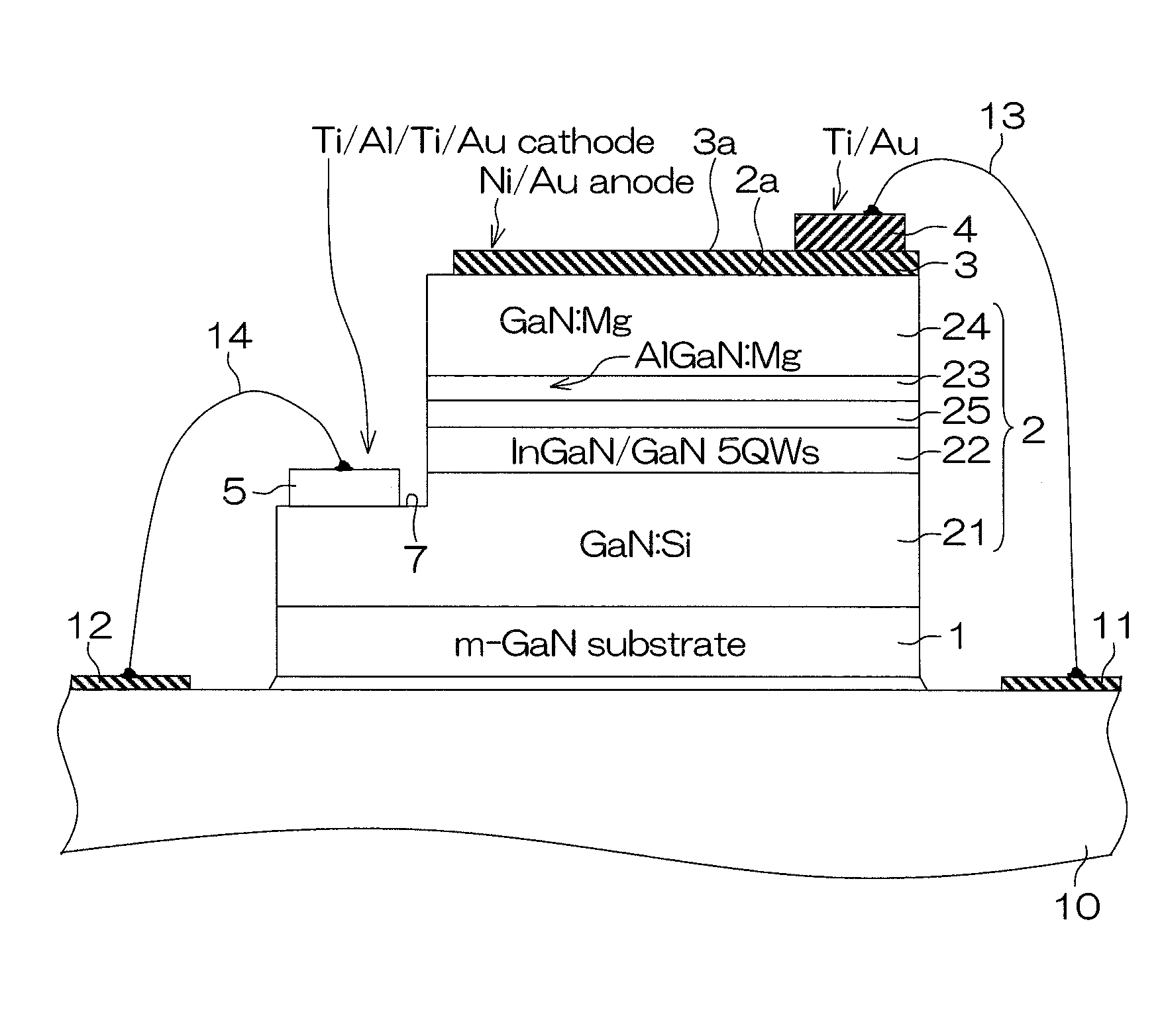
[0092]FIG. 8 is a schematic diagram for illustrating the structure of a light-emitting diode according to the present invention. Referring to FIG. 8, portions corresponding to the respective portions shown in the aforementioned FIG. 1 are denoted by the same reference numerals. According to the embodiment, a group III nitride semiconductor layered portion 2 is grown on a GaN monocrystalline substrate 1, and the GaN monocrystalline substrate 1 is thereafter removed by polishing or the like. Thus, an n-type contact layer 21 is exposed. A cathode electrode 5 is formed on the surface (the lower surface) of the exposed contact layer 21. The cathode electrode 5 is bonded (die-bonded) to a wire 12 on a support substrate 10. Thus, a light-emitting diode structure is fixed to the support substrate 10. On the other hand, an anode electrode (transparent electrode) 3 formed in contact with a surface 2a of the group III nitride semiconductor layered portion 2 on the light extraction is connected...

third embodiment

[0099]In other words, a surface 21a (a surface on a light extraction side) of the n-type contact layer 21 positioned on a side opposite to the support substrate 10 is finished into a mirror surface, similarly to the case of the On the other hand, a GaN semiconductor 2 is etched (plasma-etched, for example) until the n-type contact layer 21 is exposed from the side of the support substrate 10, and a recess 17 is formed. A cathode electrode 5 in contact with the n-type contact layer 21 is formed in the recess 17. The cathode electrode 5 and the wire 12 on the support substrate 10 are connected with each other by a metallic post 18.

[0100]Also in the structure of the embodiment, the surface 21a on the light extraction side of the group III nitride semiconductor layered portion 2 is a mirror surface, whereby light emitted from a quantum well layer 22 can be extracted outward in a hardly influenced polarization state.

fifth embodiment

[0101]FIG. 11 is a perspective view for illustrating the structure of a semiconductor laser diode which is a light-emitting device according to the present invention, and FIG. 12 is a longitudinal sectional view thereof.

[0102]A semiconductor laser diode 70 is a Fabry-Perot laser diode including a substrate 71, a group III nitride semiconductor multilayer structure 72 formed on the substrate 71 by crystal growth, an n-type electrode 73 formed to be in contact with the rear surface (the surface opposite to the group III nitride semiconductor multilayer structure 72) of the substrate 71 and a p-type electrode 74 formed to be in contact with the surface of the group III nitride semiconductor multilayer structure 72.

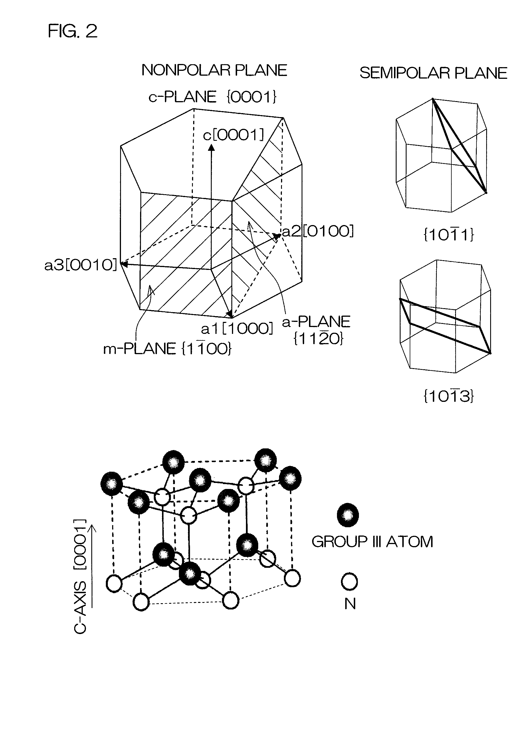
[0103]The substrate 71 is constituted of a GaN monocrystalline substrate in the embodiment. The major surface of the substrate 71 is defined by an m-plane, and the group III nitride semiconductor multilayer structure 72 is formed by crystal growth on the major surface. Theref...


PUM


Abstract

A light-emitting device includes a group III nitride semiconductor layer of a multilayer structure consisting of a group III nitride semiconductor having a major surface defined by a nonpolar plane or a semipolar plane and having at least an n-type layer and a p-type layer. A surface of the group III nitride semiconductor layer on a light extraction side is a mirror surface. The light-emitting device may further include a transparent electrode in contact with the surface of the group III nitride semiconductor layer on the light extraction side. In this case, a surface of the transparent electrode on the light extraction side is preferably a mirror surface.

Description

TECHNICAL FIELD[0001]The present invention relates to a light-emitting device (a light-emitting diode, a laser diode or the like) employing a group III nitride semiconductor.PRIOR ART[0002]A group III nitride semiconductor is a group III-V semiconductor employing nitrogen as a group V element. Typical examples of the group III nitride semiconductor include aluminum nitride (AlN), gallium nitride (GaN) and indium nitride (InN). The group III nitride semiconductor can be generally expressed as AlxInyGa1-x-yN (0≦x≦1, 0≦y≦1 and 0≦x+y≦1), and is hereinafter referred to as a “gallium nitride semiconductor” or a “GaN semiconductor”.[0003]A method of manufacturing a nitride semiconductor by growing a group III nitride semiconductor on a gallium nitride (GaN) substrate having a major surface defined by a c-plane by metal organic chemical vapor deposition (MOCVD) is known. A GaN semiconductor multilayer structure having an n-type layer and a p-type layer can be formed by applying the method, ...

Claims


Application Information

Patent Timeline
IPC IPC(8): H01L33/00H01L33/10H01L33/12H01L33/22H01L33/32H01L33/42H01L33/44H01L33/56H01L33/62
CPCB82Y20/00H01L2224/49107H01L33/20H01L33/405H01L33/42H01S5/028H01S5/0283H01S5/0425H01S5/2009H01S5/2201H01S5/3202H01S5/34333H01L33/16H01L2224/48091H01L2224/16H01L2924/3025H01L2924/00014H01L2924/00H01L2224/04042H01S5/32025H01S5/04254H01S5/4031
Inventor OKAMOTO, KUNIYOSHIOHTA, HIROAKI
Owner ROHM CO LTD
Why Eureka
Try Eureka