Organic Light Emitting Diode Display Device and Manufacturing Method Thereof

Inactive Publication Date: 2010-04-22
WINTEK CORP
View PDF4 Cites 1 Cited by
  • Summary
  • Abstract
  • Description
  • Claims
  • Application Information

AI Technical Summary

Problems solved by technology

However, a cathode made of a light-pervious material often has an inferior electron injection effect which further affects the display effect.
When the voltage applied to the cathode common OLED display device increases, the driving voltage of the thin film transistors is affected to become unstable.
As a result, the organic material layer may be sputtered and damaged during the manufacturing process, hence affecting the light emitting effect.

Method used


Image

  • Organic Light Emitting Diode Display Device and Manufacturing Method Thereof
  • Organic Light Emitting Diode Display Device and Manufacturing Method Thereof
  • Organic Light Emitting Diode Display Device and Manufacturing Method Thereof

Examples


Embodiment Construction

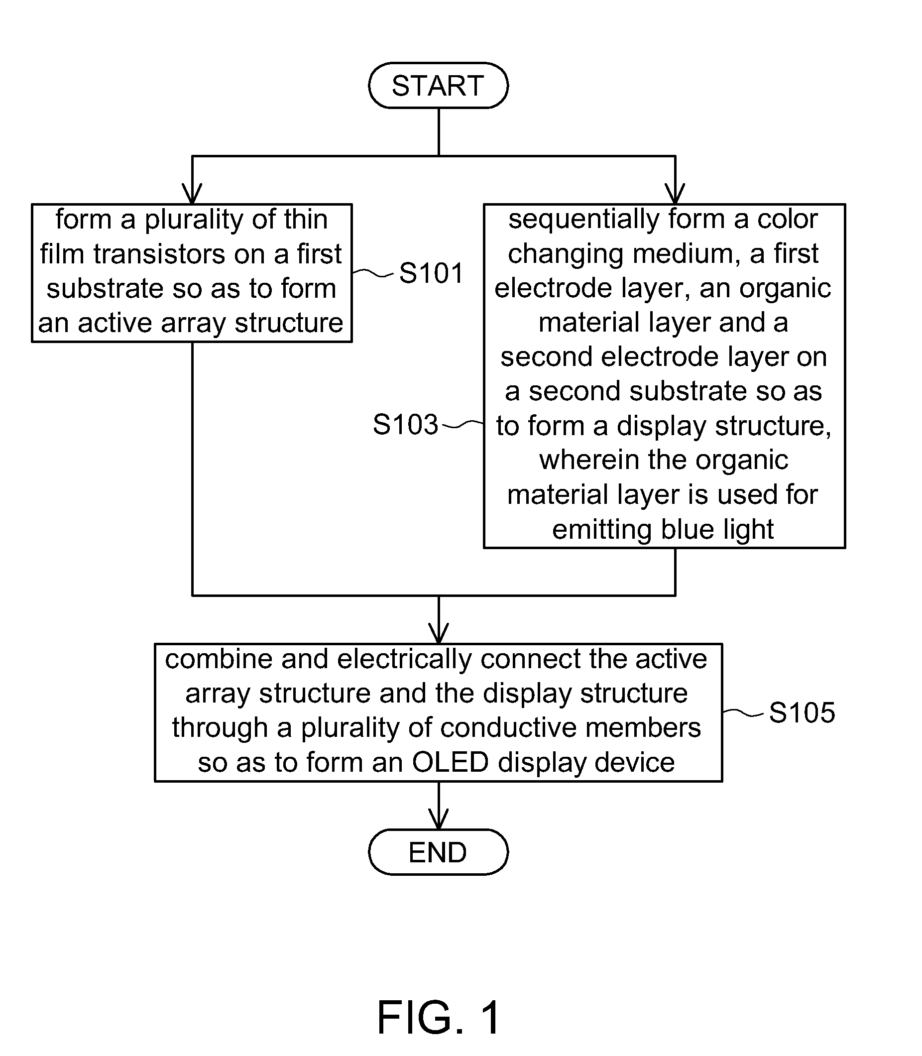
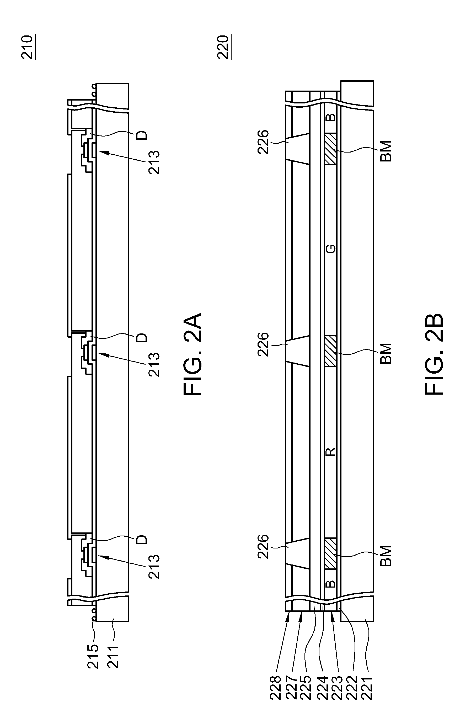
[0019]Referring to FIG. 1 and FIG. 2A, a flowchart of a manufacturing method of an OLED display device according to a preferred embodiment of the present invention is shown in FIG. 1, and a sectional view of an active array structure according to a preferred embodiment of the present invention is shown in FIG. 2A. In the step S101, several thin film transistors (TFT) 213 are formed on a surface of a first substrate 211 so as to form an active array structure 210. The thin film transistors 213 can be poly crystalline silicon thin film transistors, microcrystalline silicon thin film transistors or amorphous silicon thin film transistors.

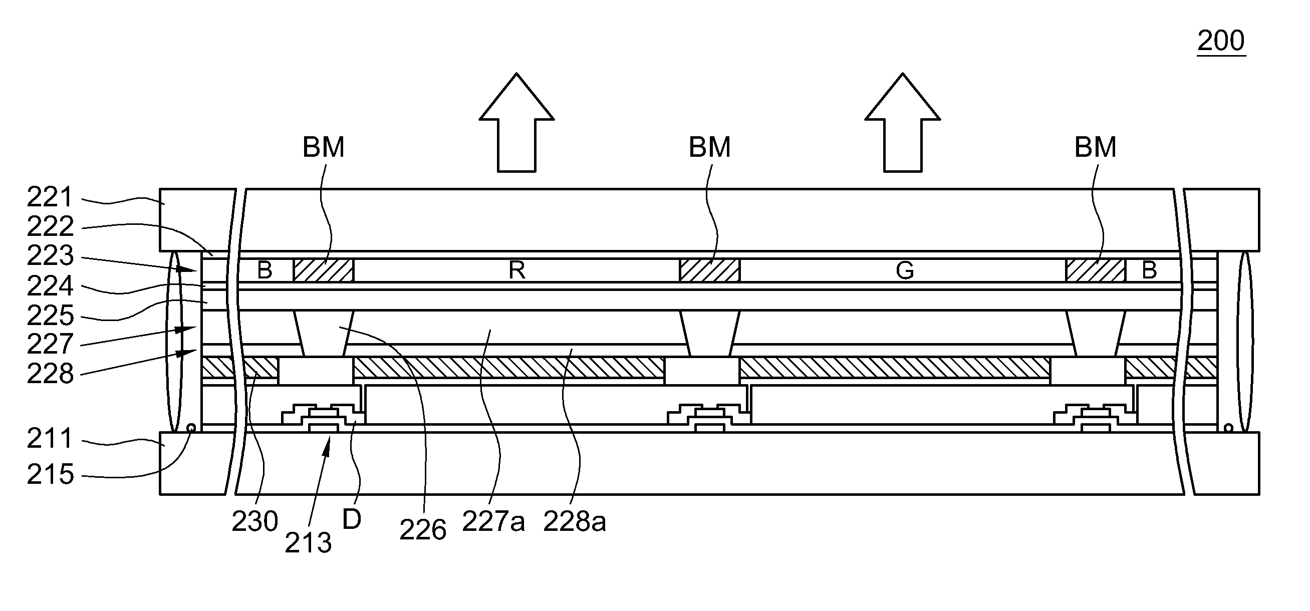
[0020]Referring to FIG. 2B, a sectional view of a display structure according to a preferred embodiment of the present invention is shown. In the step S103, an auxiliary electrode 222, a color changing medium 223, a passivation layer 224, a first electrode layer 225, an organic material layer 227 and a second electrode layer 228 are sequentially formed...


PUM


Abstract

An organic light emitting diode (OLED) display device including an active array structure, a display structure and several conductive members is provided. The active array structure includes a first substrate and several thin film transistors. The thin film transistors disposed on the first substrate has several drains. The display structure includes a second substrate, a color changing medium, a first electrode layer, an organic material layer and a second electrode layer disposed sequentially. The location of the second substrate corresponds to that of the first substrate. The color changing medium has several color blocks. The organic material layer is used for emitting blue light and includes several lighting structures electrically insulated from each other. The second electrode layer includes several electrode structures electrically insulated from each other. Each of the conductive members is combined and electrically connected to the drain of each thin film transistor and each electrode structure.

Description

[0001]This application claims the benefit of U.S. Provisional Application No. 61 / 107,411, filed Oct. 22, 2008, the subject matter of which is incorporated herein by reference.BACKGROUND OF THE INVENTION[0002]1. Field of the Invention[0003]The invention relates in general to a display device, and more particularly to an OLED display device having two substrates and a manufacturing method thereof.[0004]2. Description of the Related Art[0005]Organic light emitting diode (OLED) display devices can be divided into the bottom emission type, the top emission type and the inverted top emission type according to the light emitting direction and structure. The bottom emission type OLED display device includes a bottom substrate, an anode, an organic material layer, a cathode and a top substrate sequentially disposed. As the light emitted by the organic material layer of the bottom emission type OLED display device passes through the bottom substrate on which several thin film transistors are ...

Claims


Application Information

Patent Timeline
IPC IPC(8): G09G3/32H01L21/50
CPCG09G3/3225G09G2300/023G09G2300/0452G09G2320/0238H01L2227/323G09G2320/0666H01L27/3251H01L51/5284G09G2320/0242H10K59/127H10K59/1201H10K59/8792H10K50/865
Inventor WANG, WEN-CHUNCHANG, CHUN-CHINLIN, SHERRY
Owner WINTEK CORP
Why Eureka
Try Eureka