Aqueous dispersion for chemical mechanical polishng and chemical mechanical polishing method for semiconductor device

a technology of chemical mechanical polishing and aqueous dispersion, which is applied in the direction of polishing compositions with abrasives, chemistry apparatus and processes, and other chemical processes, can solve the problems that the polishing aqueous dispersions cannot achieve a polishing rate ratio sufficient for practical applications, and the silicon nitride film may remain or the lower layer of the silicon nitride film may be damaged, etc., to achieve the effect of increasing the polishing rate of silicon oxide film

Active Publication Date: 2010-04-22
JSR CORPORATIOON
View PDF14 Cites 28 Cited by
  • Summary
  • Abstract
  • Description
  • Claims
  • Application Information

AI Technical Summary

Benefits of technology

[0021]Since the chemical mechanical polishing aqueous dispersion according to one aspect of the invention can sufficiently increase the polishing rate of a silicon oxide film and the polishing rate of a silicon nitride film to an almost equal level, a silicon oxide film and a silicon nitride film can be simultaneously polished.

Problems solved by technology

On the other hand, most of the chemical mechanical polishing aqueous dispersions cannot polish a silicon nitride film at a practical polishing rate.
However, when using a method that dissolves a silicon nitride film by using hot phosphoric acid and removes the silicon nitride film by etching, the silicon nitride film may remain or the lower layer of the silicon nitride film may be damaged since the etching treatment is controlled based on the etching time.
However, these chemical mechanical polishing aqueous dispersions cannot achieve a polishing rate ratio sufficient for practical applications.

Method used


Image

  • Aqueous dispersion for chemical mechanical polishng and chemical mechanical polishing method for semiconductor device
  • Aqueous dispersion for chemical mechanical polishng and chemical mechanical polishing method for semiconductor device
  • Aqueous dispersion for chemical mechanical polishng and chemical mechanical polishing method for semiconductor device

Examples


examples 1 to 19

3.4 Examples 1 to 19 and Comparative Examples 1 to 12

[0105]In Examples 1 to 19 and Comparative Examples 1 to 12, the component or the concentration of the chemical mechanical polishing aqueous dispersion was changed as shown in Tables 1 to 3. The test results are also shown in Tables 1 to 3.

[0106]The chemical mechanical polishing aqueous dispersions of Examples 1 to 14 contained the colloidal silica particles of which the ratio of the major axis to the minor axis was greater than 1.3. The polishing rate ratio of the silicon nitride film to the silicon oxide film achieved by the chemical mechanical polishing aqueous dispersions of Examples 1 to 14 was sufficiently greater than 10. Therefore, the silicon nitride film can be selectively polished by chemical mechanical polishing using each of the chemical mechanical polishing aqueous dispersions of Examples 1 to 14.

[0107]The chemical mechanical polishing aqueous dispersions of Examples 15 to 19 contained the colloidal silica particles o...

first experimental example

3.5.1 First Experimental Example

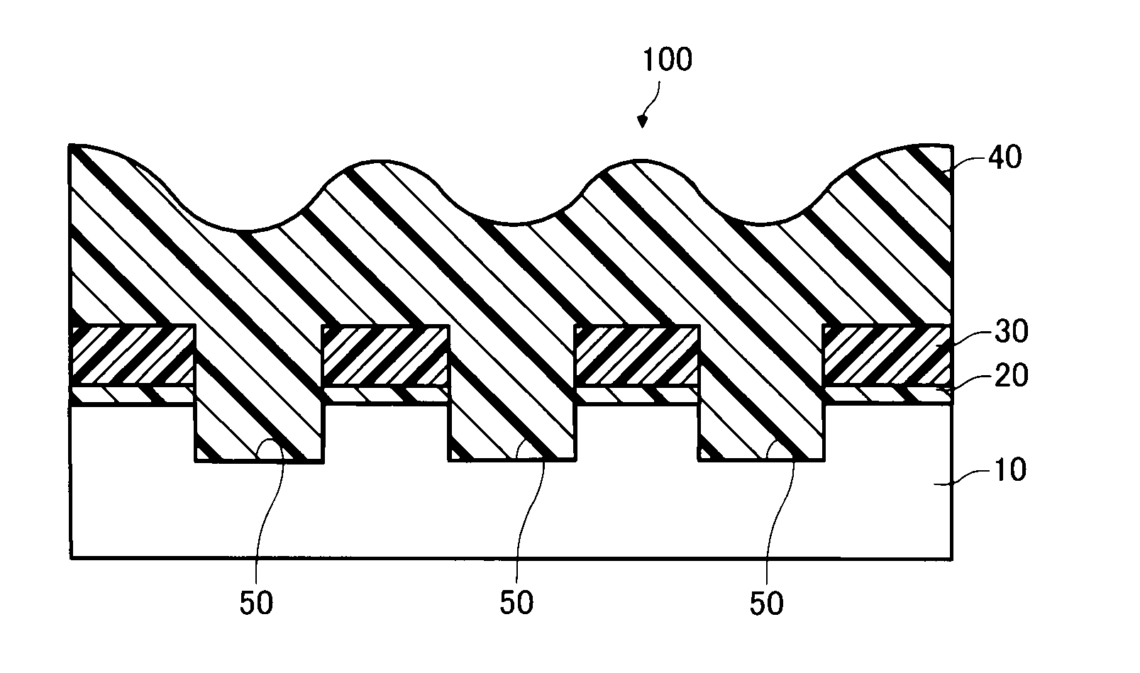
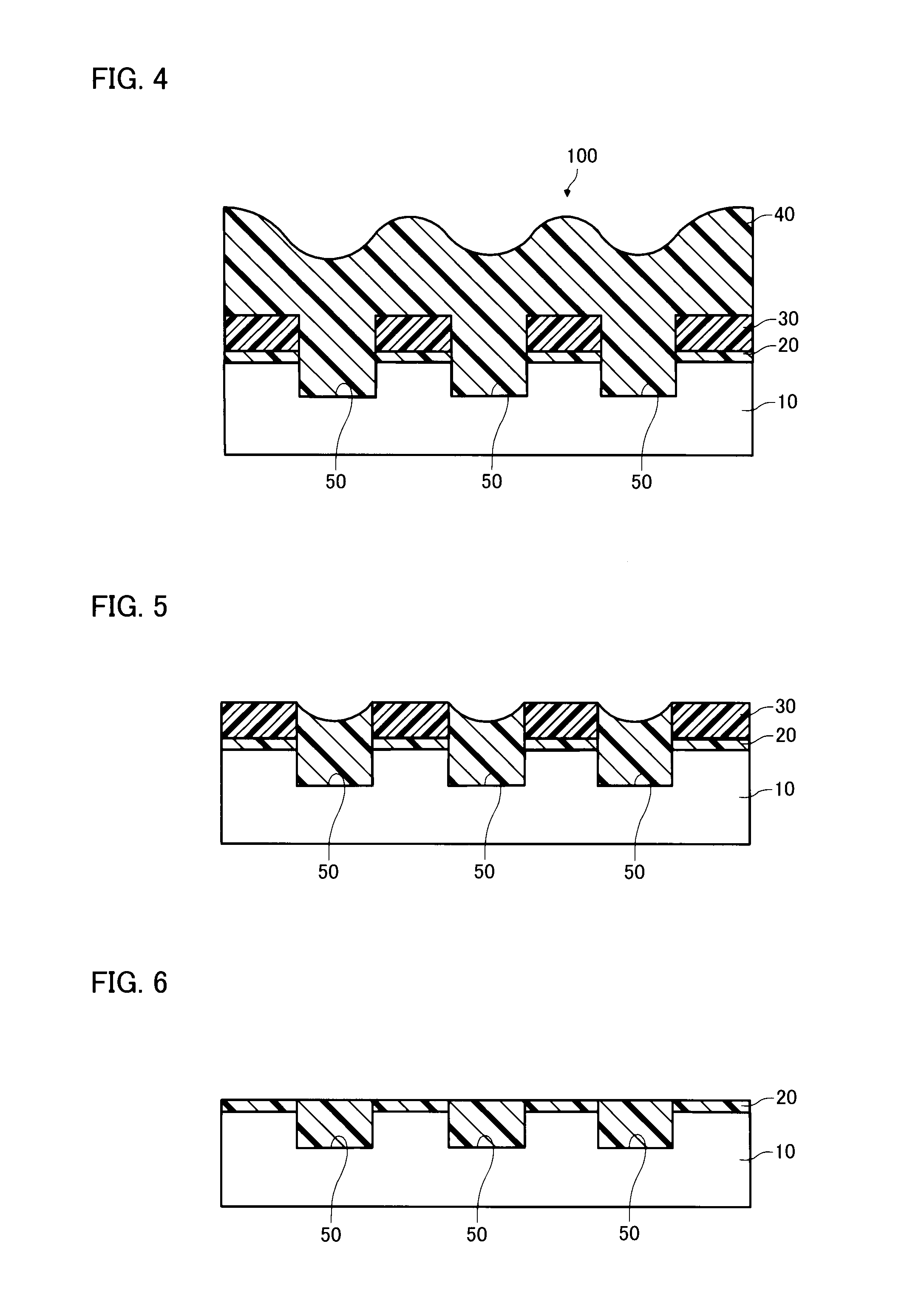
[0119]A test wafer in which a silicon nitride film was embedded was chemically and mechanically polished. Specifically, a test wafer “864CMP” (manufactured by Advanced Materials Technology Inc., the test wafer had a cross-sectional structure illustrated in FIG. 7, in which the thickness from the bottom of a polysilicon film 12 to the top of a silicon nitride film 32 was about 500 nm, the thickness of a first silicon oxide film 22 was about 10 nm, and the thickness of the silicon nitride film 32 was about 150 nm) was used as a polishing target 200.

[0120]The test wafer was preliminarily chemically and mechanically polished for 150 seconds under following “Polishing conditions 2” using “CMS4301” and CMS4302 (manufactured by JSR Corporation).

[0121]Polishing apparatus: “EPO-112” manufactured by Ebara Corporation

Polishing pad: “IC 1000 / K-Groove” manufactured by Rodel Nitta

Chemical mechanical polishing aqueous dispersion supply rate: 200 ml / min

Platen rotatio...

second experimental example

3.5.2 Second Experimental Example

[0127]A test wafer in which a silicon nitride film was embedded was chemically and mechanically polished. Specifically, a test wafer “864CMP” (manufactured by Advanced Materials Technology Inc., the test wafer had a cross-sectional structure illustrated in FIG. 10, in which the thickness from the bottom of a silicon film 14 to the top of a silicon nitride film 32 was about 500 nm, the thickness of a silicon oxide film 22 was about 10 nm, and the thickness of the silicon nitride film 32 was about 150 nm) was used as a polishing target 300.

[0128]The test wafer was preliminarily chemically and mechanically polished for 100 seconds under the above “Polishing conditions 2” using CMS4301 and CMS4302 (manufactured by JSR Corporation).

[0129]A silicon oxide film 42 formed on the silicon nitride film 32 was almost completely removed by chemical mechanical polishing, as illustrated in FIG. 11. The thickness of the silicon oxide film 42 formed on the silicon nit...


PUM

PropertyMeasurementUnit
particle sizeaaaaaaaaaa
pHaaaaaaaaaa
mass ratioaaaaaaaaaa

Abstract

A chemical mechanical polishing aqueous dispersion includes (A) colloidal silica having an average particle size calculated from the specific surface area determined by the BET method of 10 to 60 nm, (B) an organic acid having two or more carboxyl groups and one or more hydroxyl groups in one molecule, and (C) a quaternary ammonium compound shown by the following general formula (1),
wherein R1 to R4 individually represent hydrocarbon groups, and M represents an anion, the chemical mechanical polishing aqueous dispersion having a pH of 3 to 5.

Description

TECHNICAL FIELD[0001]The present invention relates to a chemical mechanical polishing aqueous dispersion and a chemical mechanical polishing method for a semiconductor device using the chemical mechanical polishing aqueous dispersion.BACKGROUND ART[0002]Various chemical mechanical polishing (hereinafter referred to as “CMP”) aqueous dispersions that can chemically and mechanically polish a silicon oxide film, a polysilicon film, or the like at a practical polishing rate have been developed. On the other hand, most of the chemical mechanical polishing aqueous dispersions cannot polish a silicon nitride film at a practical polishing rate. Therefore, a method that removes a silicon oxide film formed on a silicon nitride film by CMP using the silicon nitride film as a stopper has been used. The silicon nitride film used as the stopper must be removed after removing the silicon oxide film.[0003]However, when using a method that dissolves a silicon nitride film by using hot phosphoric aci...

Claims


Application Information

Patent Timeline
Patent Type & Authority Applications(United States)
IPC IPC(8): H01L21/302C09K13/00
CPCC09G1/02H01L21/31053C09K3/1463C09K3/14H01L21/304
Inventor MATSUMOTO, TAICHIUENO, TOMIKAZUANDOU, MICHIAKI
Owner JSR CORPORATIOON
Why Eureka
Try Eureka