Single-sided lateral-field and phototransistor-based optoelectronic tweezers

Active Publication Date: 2010-04-29
RGT UNIV OF CALIFORNIA
View PDF17 Cites 64 Cited by
  • Summary
  • Abstract
  • Description
  • Claims
  • Application Information

AI Technical Summary

Benefits of technology

[0018]We have designed, fabricated, and demonstrated a new device for producing optically-controlled dielectrophoretic forces. Previous demonstrations of optically-induced dielectrophoresis, in optoelectronic tweezers (OET) devices, have used electrical fields that are perpendicular to the plane of the device, causing irregular or rod-shaped particles to align to the vertical electric field. Our new device, single-sided lateral-field optoelectronic tweezers (LOET), uses photosensitive electrode arrays to create optically-induced dielectrophoretic forces in an electric field that is parallel to the pl

Problems solved by technology

However, it is sometimes advantageous to have an electric field

Method used


Image

  • Single-sided lateral-field and phototransistor-based optoelectronic tweezers
  • Single-sided lateral-field and phototransistor-based optoelectronic tweezers
  • Single-sided lateral-field and phototransistor-based optoelectronic tweezers

Examples


example 1

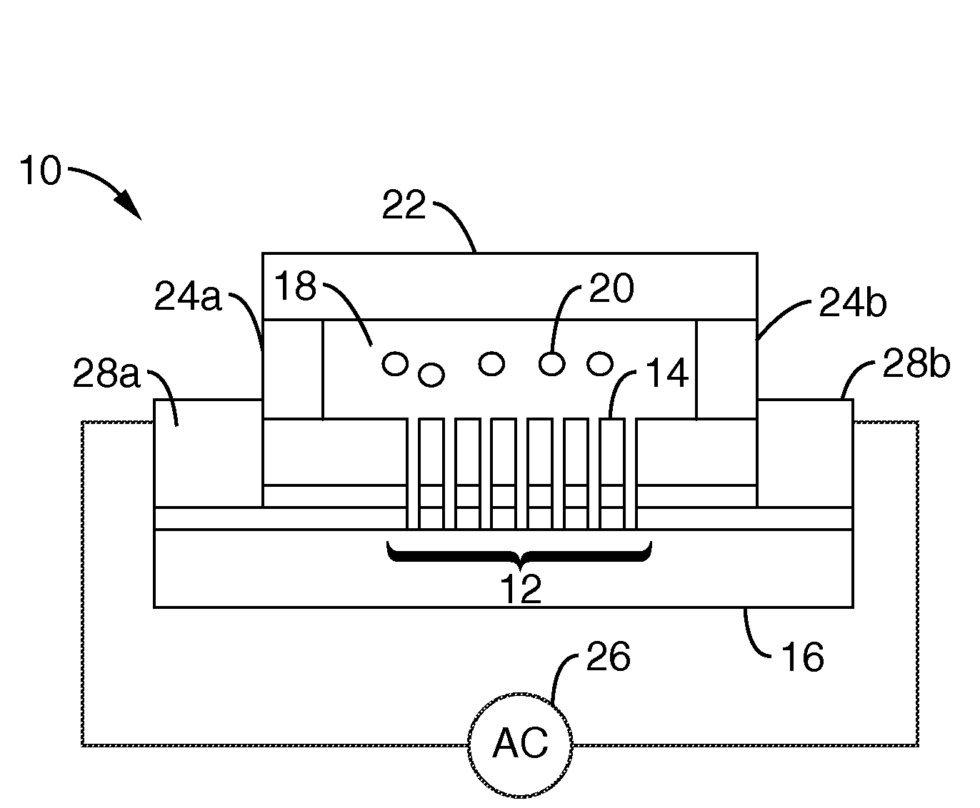
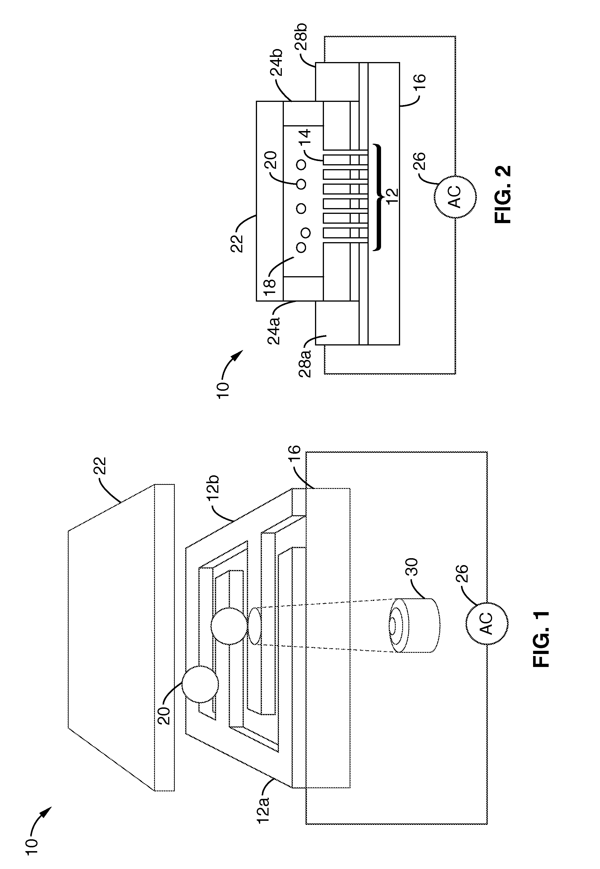
[0055]An interdigitated LOET device as illustrated in FIG. 1 and FIG. 2 was created by depositing 100-nm of ITO on an insulating substrate 16. Other conductive materials may also be used. A 50-nm layer of highly-doped a-Si:H is deposited over the ITO, followed by a 1-μm-thick layer of intrinsic a-Si:H 14. Both a-Si:H layers are deposited by plasma-enhanced chemical vapor deposition. Electrode patterns 12 were etched into the a-Si:H layers by reactive ion etching. The patterns are transferred to the ITO layer by a wet acid etch. Electrical contact pads 28 were created by etching the a-Si:H layers down to the ITO layer, and adding conductive epoxy or another conductive material over the exposed ITO layer.

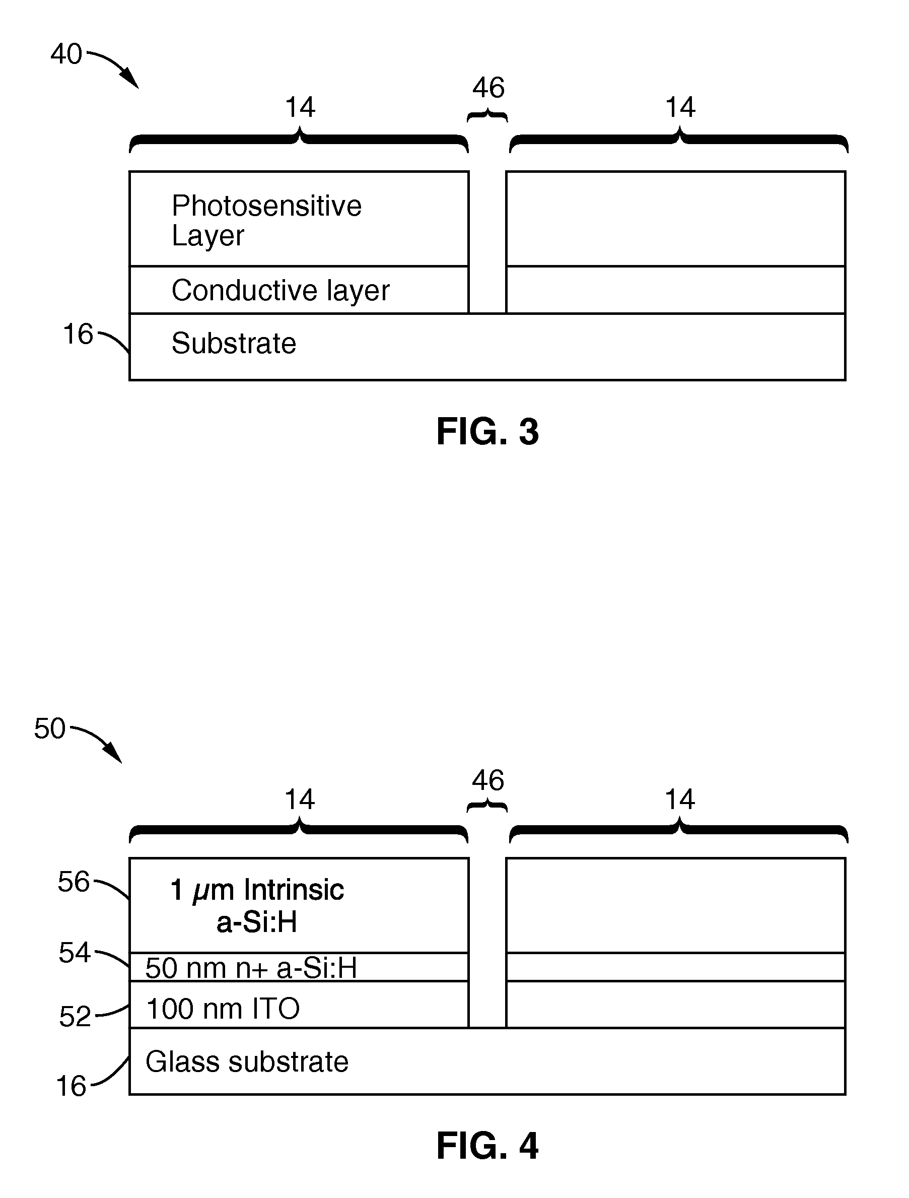
[0056]Referring now to FIG. 3, in a generalized embodiment 40, the device may comprise any type of conductive material 42 on the substrate 16, topped by a photosensitive layer 44 of varying thickness, with individual devices spaced apart by an electrode gap 46.

example 2

[0057]In a specific embodiment 50 shown in FIG. 4, the electrodes 14 comprise a 100-nm-thick indium-tin-oxide (ITO) layer 52 on a glass substrate 16, topped by a 50-nm-thick layer 54 of highly doped hydrogenated amorphous silicon (a-Si:H), and a 1-μm-thick layer 56 of intrinsic a-Si:H. Alternative materials can be used as long as they retain the indicated material properties shown in FIG. 3 (i.e., conductive or photosensitive).

[0058]In one embodiment, the inventive LOET device utilizes 10-μm-wide electrodes, with a 20-μm gap 46 between electrodes. However, other electrode sizes and gaps between the electrodes may be utilized.

[0059]Referring now to FIG. 3, FIG. 5 and FIG. 6, various alternative configurations of the generalized LOET structure can be utilized to improve the electric field characteristics of the LOET device. For example, in the embodiment 60 shown in FIG. 5A, the conductive layer 42 may be undercut. In the embodiment 70 shown in FIG. 5B, the conductive layer 42 is enve...

example 3

[0060]Referring to FIG. 7, illumination of the electrodes in the inventive LOET structure and various embodiments described above causes actuation of OET force, as in a conventional OET device. Significantly, however, as illustrated by FIG. 7, the electric field in the inventive LOET device is parallel to the plane of the electrodes for electrodes that have no undercut of the conductive layer as shown in FIG. 7A, electrodes with an undercut conductive layer as shown in FIG. 7B, electrodes with a conductive layer enveloped by photosensitive layer as shown in FIG. 7C, and electrodes with a thin insulating passivation layer in the gap between the electrodes as shown in FIG. 7D. In FIG. 7A, the high-electric-field regions at the edge of the electrodes are undesirable—the regions above the center of the electrodes are the desired high-electric-field regions. FIG. 7B through FIG. 7D show that the corresponding designs reduce the electric field at the electrode edges.


PUM

PropertyMeasurementUnit
Dielectric polarization enthalpyaaaaaaaaaa
Electrical conductoraaaaaaaaaa
Photoconductivityaaaaaaaaaa

Abstract

Described herein are single-sided lateral-field optoelectronic tweezers (LOET) devices which use photosensitive electrode arrays to create optically-induced dielectrophoretic forces in an electric field that is parallel to the plane of the device. In addition, phototransistor-based optoelectronic tweezers (PhOET) devices are described that allow for optoelectronic tweezers (OET) operation in high-conductivity physiological buffer and cell culture media.

Description

CROSS-REFERENCE TO RELATED APPLICATIONS[0001]This application claims priority from, and is a 35 U.S.C. §111(a) continuation of, PCT international application serial number PCT / US2008 / 058701, filed on Mar. 28, 2008, incorporated herein by reference in its entirety, which claims priority to U.S. provisional patent application Ser. No. 60 / 943,103 filed on Jun. 11, 2007, incorporated herein by reference in its entirety, U.S. provisional patent application Ser. No. 60 / 909,845 filed on Apr. 3, 2007, incorporated herein by reference in its entirety, and U.S. provisional patent application Ser. No. 60 / 908,452, filed on Mar. 28, 2007, incorporated herein by reference in its entirety.[0002]This application is also related to PCT International Publication No. WO 2008 / 119066 published on Oct. 2, 2008, incorporated herein by reference in its entirety.STATEMENT REGARDING FEDERALLY SPONSORED RESEARCH OR DEVELOPMENT[0003]This invention was made with Government support under Grant No. NCC 2-1364, aw...

Claims


Application Information

Patent Timeline
IPC IPC(8): G01N27/447H01L31/11H01L31/18
CPCB82Y20/00B82Y15/00
Inventor OHTA, AARONCHIOU, PEI-YUHSU, HSAN-YINJAMSHIDI, ARASHWU, MING-CHIANGNEALE, STEVEN L.
Owner RGT UNIV OF CALIFORNIA
Why Eureka
Try Eureka