Nano-devices and methods of manufacture thereof

a technology of nano-devices and manufacturing methods, applied in the field of nano-devices, can solve the problems of poor electrical contact between the nano-wire and the second substrate, mechanical damage to the nano-wire, and poor control of the number of nano-wires transferred and the position of the transferred nano-wires on the second substra

Inactive Publication Date: 2010-05-06
GENERAL ELECTRIC CO
View PDF16 Cites 28 Cited by
  • Summary
  • Abstract
  • Description
  • Claims
  • Application Information

AI Technical Summary

Problems solved by technology

These methods of transferring the nanowires generally have drawbacks in that there is poor control of the number of nanowires transferred and the position of the transferred nanowires on the second substrate.
In a...

Method used


Image

  • Nano-devices and methods of manufacture thereof
  • Nano-devices and methods of manufacture thereof
  • Nano-devices and methods of manufacture thereof

Examples


example

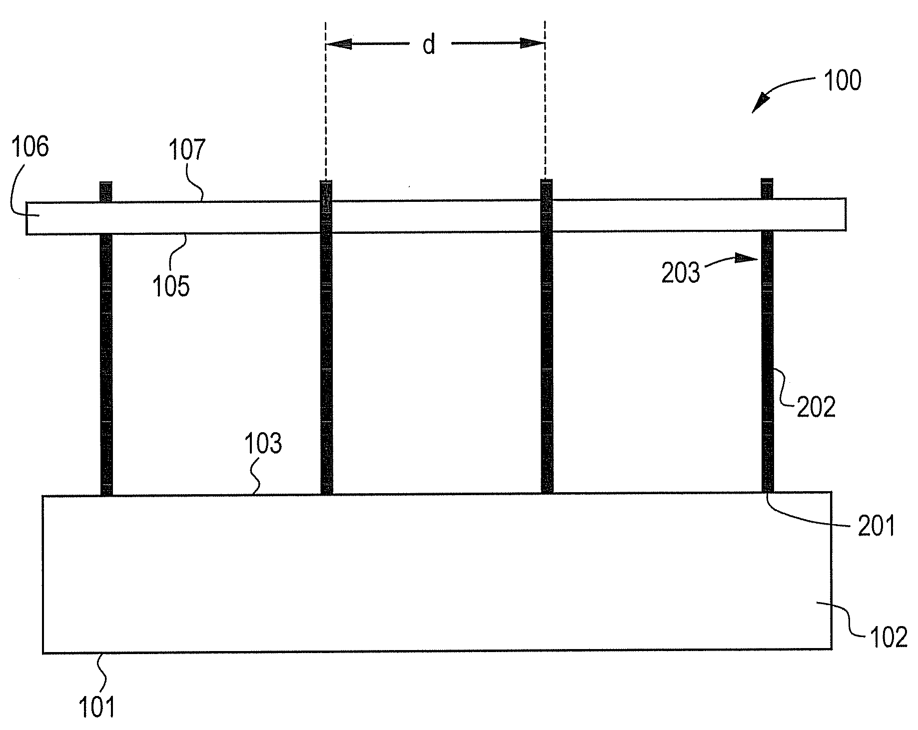
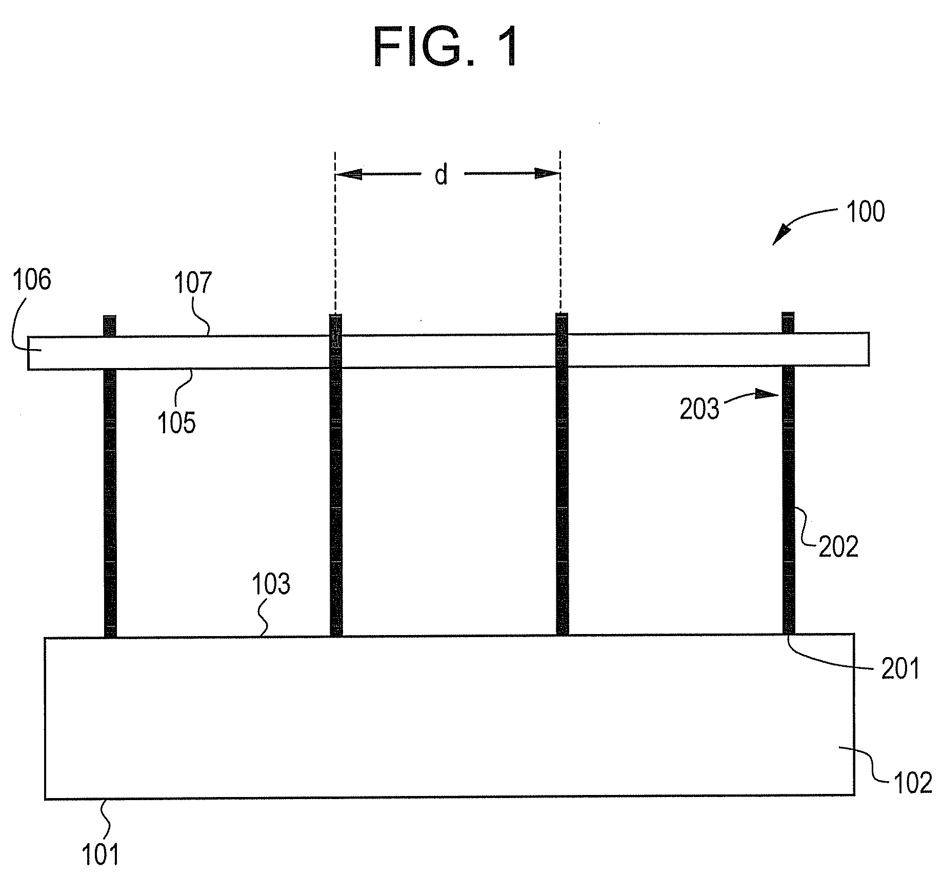
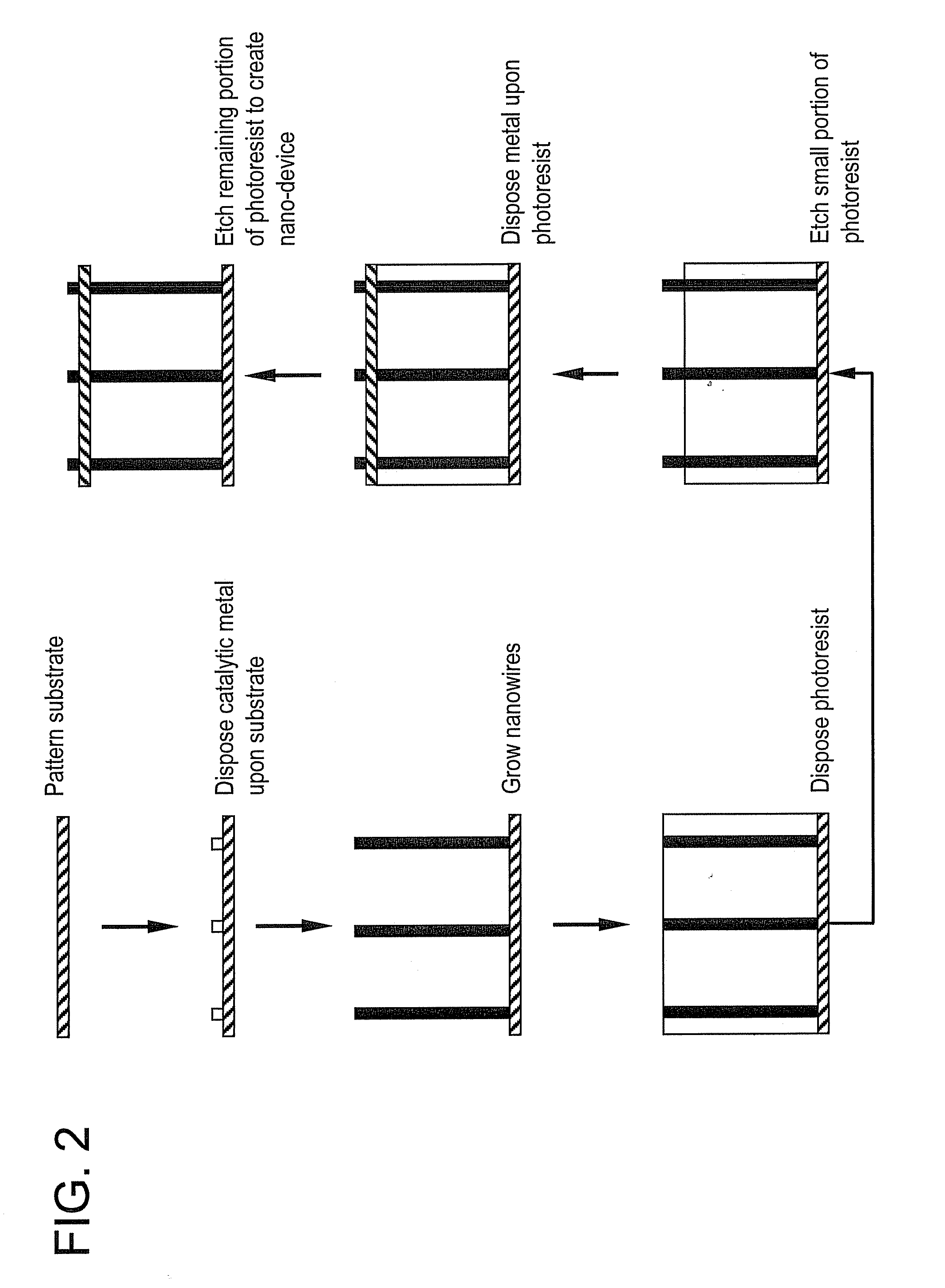
[0053]This example was conducted to demonstrate a method for manufacturing the nano-device disclosed herein. A silicon wafer was used as the substrate. A pattern of 0.7 to 0.8 micrometer diameter gold catalyst dots was disposed on the substrate using photolithography. The gold catalyst was 5 nm thick and was deposited by electron beam evaporation onto a double layer liftoff photoresist structure. The liftoff was performed in standard resist solvents (acetone and N-methyl pyrrolidone based solvents). Silicon nanowires having a length of approximately 3 micrometers were grown perpendicular to the silicon wafer surface using thermal chemical vapor deposition. The wires were then coated with amorphous silicon and indium tin oxide (ITO), giving the nanowires a rough grain structure observed in the SEM image shown in the FIG. 5.

[0054]A □micrometer thick layer of photoresist was spin coated onto the substrate containing the nanowire array, filling in the gaps between wires and forming a ...


PUM


Abstract

Disclosed herein is a nanodevice. Disclosed herein too is a method of manufacturing a nanodevice. In one embodiment the nanodevice includes a first substrate; a second substrate; a nanowire; the nanowire contacting the first substrate and the second substrate; the nanowire comprising a metal, a semi-conductor or a combination thereof.

Description

BACKGROUND OF THE INVENTION[0001]This disclosure relates to nano-devices and to methods of manufacture thereof.[0002]Fabrication processes for the manufacture of nano-devices involve growing nanowires on a first substrate and then transferring them to a second substrate to facilitate the manufacturing of the nano-device. Transferring methods such as drop casting of nanowires suspended in a solution, mechanical rubbing of the first substrate that contains the nanowires against the second substrate, transferring nanowires using nanomanipulation methods, and the like, have been attempted. These methods of transferring the nanowires generally have drawbacks in that there is poor control of the number of nanowires transferred and the position of the transferred nanowires on the second substrate. In addition, the transferring often causes mechanical damage to the nanowires and there is poor electrical contact between the nanowires and the second substrate. These methods are therefore not ...

Claims


Application Information

Patent Timeline
IPC IPC(8): H01L31/0352H01L21/20H01L29/06
CPCB81B1/00B81B2201/0214B81B2201/0292B82Y10/00B82Y15/00B82Y30/00H01L21/02381H01L21/02521H01L21/02532H01L21/02645H01L21/02653H01L29/0665H01L29/0673H01L29/0676H01L31/035227H01L31/03529
Inventor TSAKALAKOS, LOUCASKOREVAAR, BASTIAAN ARIEBALCH, JOLEYN EILEENFRONHEISER, JODYLI, BOZRIBI, ANIS
Owner GENERAL ELECTRIC CO
Why Eureka
Try Eureka